Semiconductor device having an internal-field-guarded active region

a technology of active region and shielding effect, which is applied in the direction of shielding device, basic electric element, electrical apparatus, etc., can solve the problems of red shift of light emission, achieve low internal absorption of photons, reduce the effect of polarization shielding effect, and achieve special strong advantageous effect

Active Publication Date: 2018-09-13
TECHNICAL UNIVERSITY OF BERLIN
View PDF0 Cites 0 Cited by
  • Summary
  • Abstract
  • Description
  • Claims
  • Application Information

AI Technical Summary

Benefits of technology

[0033]A thickness of the polarization guard layers is preferably at least one monolayer of a guard layer material having the first or third material composition. A selection of the thickness of the polarization guard layers in the design phase of the semiconductor device can be based on the goal of a desired fine-tuning of the energy of optical transitions by inducing, in a manner controllable by the layer design, a band bending within the active layer of the active layer stack. An upper limit of the thickness of the polarization guard layers does not exist in the sense that the polarization shielding effect could be reduced or even lost beyond a certain thickness of the polarization guard layers. This is not the case. The polarization guard layers on different sides of the active region can even have different thicknesses. Therefore, the thickness can be determined based on application requirements of a particular device design. In some examples, the thickness of the polarization guard layers is not more than 1 micrometer. In other embodiments, the thickness is at most 100 nanometer. Further embodiments have polarization guard layers with a thickness that is 50 nanometer or less.
[0034]In some embodiments, a thickness of the polarization guard layer on at least one of the opposite sides of the active region is either smaller or at most equal to a thickness of the active layer. In optical device applications, since the active layer is typically thin, this group of embodiments achieves a particularly low internal absorption of photons that are either generated or to be absorbed in the active region. In those embodiments that have a smaller thickness of the at least one polarization guard layer in comparison with the active layer, this advantageous effect can be made particularly strong. This can be attributed to a blue shift of allowed optical transitions in the polarization guard layer compared to those in the active layer. Since the polarization guard layer is of the same material composition as the active layer, a smaller thickness of the polarization guard layer in comparison with the active layer increases the energy gap between the states involved in optical transitions in the polarization guard layer beyond that in the active layer. Thus, a degree of light transmission of the polarization guard layer for photons generated in the active layer can be even further increased in comparison with a polarization guard layer of a thickness equal to that of the active layer.

Problems solved by technology

Furthermore, the band bending and resulting spatial separation of electrons and holes result in a red shift of light emission in comparison with the so-called flat-band case, in which no electric fields are present.

Method used


Image

  • Semiconductor device having an internal-field-guarded active region
  • Semiconductor device having an internal-field-guarded active region
  • Semiconductor device having an internal-field-guarded active region

Examples


Embodiment Construction

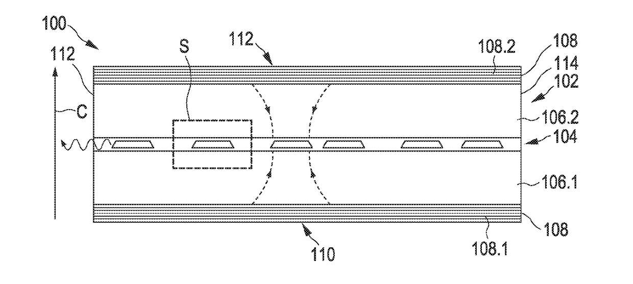
[0060]FIG. 1 is a schematic cross-sectional view of an embodiment of a quantum-dot semiconductor device 100 forming a light emitter. Reference is made in parallel to FIG. 2, which shows an enlarged view of a section S outlined by a dashed line in FIG. 1.

[0061]The quantum dot semiconductor device 100 comprises a layer sequence 102 formed by a number of polar semiconductor material layers, which will be described in the following. The semiconductor material layers are group-III nitride semiconductors and each have a hexagonal crystal structure. The layer sequence 102 consists of semiconductor material layers that each has a crystal axis pointing in a direction c indicated by a vertical arrow in FIG. 1. The c direction also forms the stacking direction of the layer sequence 102. Typically, the layer sequence 102 is fabricated by epitaxial growth, the growth direction of the layer sequence 102 thus being the c direction.

[0062]Specifically, the layer sequence 102 consists of the followin...


PUM


Abstract

A semiconductor device comprises a layer sequence formed by a plurality of polar single crystalline semiconductor material layers that each has a crystal axis pointing in a direction of crystalline polarity and a stacking direction of the layer sequence. A core layer sequence is formed by an active region made of an active layer stack or a plurality of repetitions of the active layer stack. The active layer stack has an active layer having a first material composition associated with a first band gap energy, and carrier-confinement layers embedding the active layer on at least two opposite sides thereof, having a second material composition associated with a second band gap energy larger than the first band gap energy. A pair of polarization guard layers is arranged adjacent to the active region and embedding the active region on opposite sides thereof.

Description

CROSS REFERENCE TO RELATED APPLICATION[0001]This application claims priority under 35 USC § 119 to European Patent Application No. 17160160.2 filed on Mar. 9, 2017, which application is hereby incorporated by reference in its entirety.TECHNICAL FIELD[0002]The present invention relates to a semiconductor device.BACKGROUND OF THE INVENTION[0003]Polarity in semiconductor materials arises from their crystal structure, and potentially from lattice distortion of the crystal lattice caused in particular by strained crystal lattices in semiconductor heterostructures.[0004]Examples of polar semiconductors are compound semiconductors of hexagonal crystal structure, which have a polar axis along their c-direction and compound semiconductors of zincblende structure, which have a polar axis along their [111] direction. The following introduction will concentrate on hexagonal polar semiconductors as a non-limiting example.[0005]Compound semiconductors of hexagonal crystal structure have constitue...

Claims


Application Information

Patent Timeline
Patent Type & Authority Applications(United States)
IPC IPC(8): H01L33/06H01L33/32
CPCH01L33/32H01L33/06H01L29/417H01L29/78H01L33/007H01L33/04H01L33/16H01L33/20H01L2933/0083
Inventor PAHN, GERALDCALLSEN, GORDONWESTERKAMP, STEFFEN
Owner TECHNICAL UNIVERSITY OF BERLIN
Why Eureka
Try Eureka