Semiconductor structure and fabrication method thereof

a technology of semiconductors and semiconductors, applied in the direction of semiconductor devices, electrical equipment, radio frequency controlled devices, etc., can solve the problems of difficult integration of ccd image sensors with other devices, too large power consumption of ccd image sensors,

Active Publication Date: 2018-09-20
SEMICON MFG INT (SHANGHAI) CORP +1
View PDF0 Cites 9 Cited by
  • Summary
  • Abstract
  • Description
  • Claims
  • Application Information

AI Technical Summary

Problems solved by technology

CCD image sensors have the advantages of high sensitivity and low noise, but CCD image sensors are difficult to be integrated with other devices, and the power consumption of a CCD image sensor is too large.

Method used


Image

  • Semiconductor structure and fabrication method thereof
  • Semiconductor structure and fabrication method thereof
  • Semiconductor structure and fabrication method thereof

Examples


Embodiment Construction

[0013]Reference will now be made in detail to the exemplary embodiments of the disclosure, which are illustrated in the accompanying drawings. Wherever possible, the same reference numbers will be used throughout the drawings to refer to the same or similar parts.

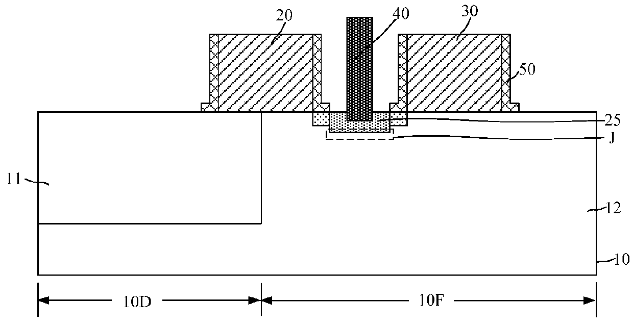
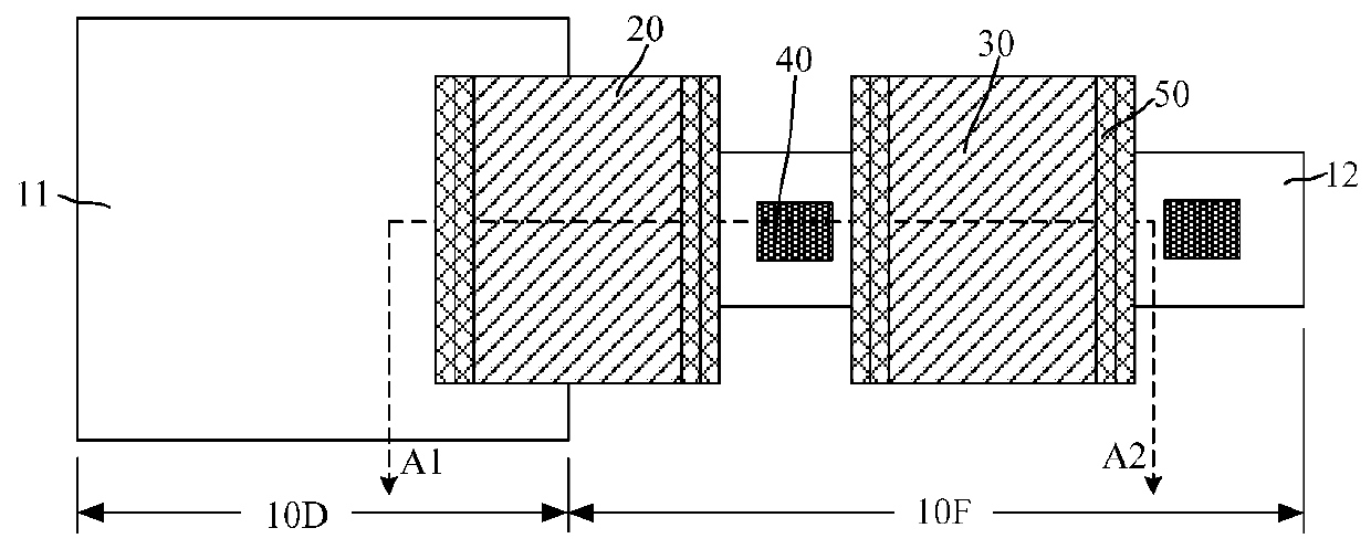
[0014]The performance of the pixel structure of a complementary metal oxide image sensor (CIS) needs to be improved. FIG. 1 illustrates a top view of a semiconductor structure, and FIG. 2 illustrates a schematic cross-sectional view of the structure along the cutting line A1A2 of FIG. 1.

[0015]As shown in FIGS. 1 and 2, the exemplary semiconductor structure is an N-type 4T pixel structure. The semiconductor structure includes a substrate 10 (shown in FIG. 2), and the substrate 10 is P-type doped. The substrate 10 includes a photosensitive region 10D and a floating diffusion region 10F adjacent to the photosensitive region, and the photosensitive region 10D is used to form a photo diode (PD). The semiconductor structure furth...


PUM

PropertyMeasurementUnit
semiconductor structureaaaaaaaaaa
photosensitiveaaaaaaaaaa
thicknessaaaaaaaaaa

Abstract

A semiconductor structure and a fabrication method are provided. The fabrication method includes: providing a substrate, containing first doping ions and including a pixel region for forming a pixel structure; forming a deeply doped region, in the photosensitive region of the substrate and containing second doping ions; forming a floating diffusion area in the floating diffusion region of the substrate and containing third doping ions; forming a gate structure on the substrate at the junction of the photosensitive region and the floating diffusion region; forming a sidewall film covering the gate structure and the substrate; forming a sidewall spacer; forming a first doped region in the floating diffusion region on one side of the gate structure; forming a metal connection layer on the first doped region; forming an interlayer dielectric layer on the substrate; and forming a source/drain contact plug in the interlayer dielectric layer.

Description

CROSS-REFERENCES TO RELATED APPLICATIONS[0001]This application claims the priority of Chinese patent application No. 201710163795.1, filed on Mar. 17, 2017, the entirety of which is incorporated herein by reference.FIELD OF THE DISCLOSURE[0002]The present disclosure generally relates to the field of semiconductor manufacturing technologies and, more particularly, relates to a semiconductor structure and a fabrication method thereof.BACKGROUND[0003]Image sensors are usually used to convert an optical signal into a corresponding electrical signal. The image sensor may include complementary metal oxide image sensor (CMOS Image Sensor, CIS) and charge coupled device (CCD) image sensor. CCD image sensors have the advantages of high sensitivity and low noise, but CCD image sensors are difficult to be integrated with other devices, and the power consumption of a CCD image sensor is too large. In contrast, CIS has the advantages of simple processing, easy integration with other devices, sma...

Claims


Application Information

Patent Timeline
Patent Type & Authority Applications(United States)
IPC IPC(8): H01L27/146H01L21/266
CPCH01L27/14689H01L27/14612H01L21/266H01L27/14636H01L27/146H01L27/14605H01L27/14683
Inventor QI, DE KUI
Owner SEMICON MFG INT (SHANGHAI) CORP
Why Eureka
Try Eureka