Solid-state image-capturing device and method for driving solid-state image-capturing device

a solid-state image and image-capturing technology, applied in the direction of color television, radio control devices, television systems, etc., can solve the problems of increasing the size of the pixel circuit, the inability to obtain analog gradation of the signal, and the increase of the number of pixels, so as to reduce the number of structural elements that constitute each pixel circuit, the effect of reducing the readout time and suppressing the frame ra

Active Publication Date: 2018-09-27
PANASONIC INTELLECTUAL PROPERTY MANAGEMENT CO LTD
View PDF0 Cites 8 Cited by
  • Summary
  • Abstract
  • Description
  • Claims
  • Application Information

AI Technical Summary

Benefits of technology

[0021]Also, a series of operations of resetting the voltage of the avalanche photodiode, performing exposure, and transferring the electric charges generated by the avalanche photodiode to the analog memory are simultaneously performed on a plurality of rows or all rows. Accordingly, the voltages of the analog memories stored in the preceding frame are read out for each row in the current frame, and thus the readout time can be apparently eliminated, and the reductio

Problems solved by technology

On the other hand, in an environment in which the number of photons is large, because the output signal is saturated, there is a problem in that the analog gradation of the Signal cannot obtained even when a plurality of incident photons are incident.
However, the conventional example disclosed in U.S. Pat. No. 8,822,900 requires output circuit 910 for the electric charge accumulation mode and output circuit 920 for

Method used


Image

  • Solid-state image-capturing device and method for driving solid-state image-capturing device
  • Solid-state image-capturing device and method for driving solid-state image-capturing device
  • Solid-state image-capturing device and method for driving solid-state image-capturing device

Examples


embodiment 1

Configuration of Pixel Circuit

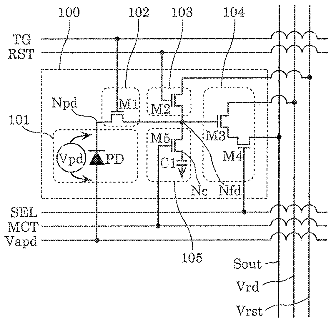
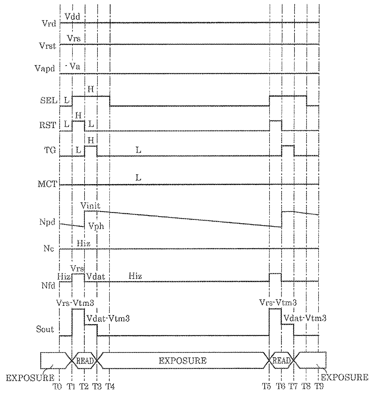
[0050]FIG. 1 is a circuit diagram showing an example of a configuration of pixel circuit 100. In pixel circuit 100, an avalanche photodiode is used as the photoelectric conversion element.

[0051]Pixel circuit 100 includes light receiver 101, transfer circuit 102, reset circuit 103, output circuit 104, and analog memory 105.

[0052]Light receiver 101 includes avalanche photodiode PD to which voltage Vpd is applied by bias terminal voltage Vapd and the initial voltage of node Npd.

[0053]Transfer circuit 102 includes transfer transistor M1 that transfers electric charges generated in node Npd through photoelectric conversion performed by avalanche photodiode PD to floating diffusion region Nfd (hereinafter, referred to simply as FD region) according o control signal TG.

[0054]Reset circuit 103 includes reset transistor M2 that selectively supplies reset voltage Vrst to all or any one of FD region Nfd, node Npd, and node Nc according to control signal RST so as ...

embodiment 2

[0162]In Embodiment 2, a description will be given of a solid-state image-capturing device that includes the pixel circuit according to Embodiment 1.

Control Signal and Buffer Circuit Configuration for Global Electronic Shutter Driving

[0163]FIG. 11 is a block diagram showing an example of a configuration of a relevant part of solid-state image-capturing device 600c that includes a plurality of pixel circuits. As the pixel circuits, for example, pixel circuits 100 as shown in FIG. 1 can be used.

[0164]Solid-state image-capturing device 600c includes: pixel array 601 that includes a plurality of pixel circuits 100 that are arranged in rows and columns; buffer circuit 602; and timing generation circuit 609. FIG. 11 shows, as an example, a configuration of two rows and two columns in solid-state image-capturing device 600c. Hereinafter, the structural elements in the i-th row will be indicated by a subscript [i], the structural elements in the j-th column will be indicated by a subscript ...

embodiment 3

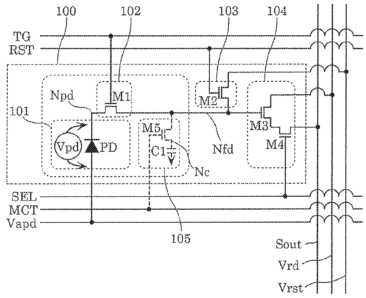
[0210]In Embodiment 3, a solid-state image-capturing device that binarizes and digitally outputs the voltage generated by the pixel circuits will be described by taking another example.

[0211]FIG. 15 is a circuit diagram showing an example of a configuration of pixel circuit 110. Pixel circuit 110 and pixel circuit 100 in FIG. 1 are common in that avalanche photodiode PD is used as a photoelectric conversion element, while being different in that analog memory 105 is omitted in pixel circuit 110. It is sufficient that pixel circuit 110 is a pixel circuit that reads out an analog signal obtained through multiplication of the electric charges. In a yet another example of pixel circuit 110, transfer circuit 102 may be further omitted and avalanche photodiode PD and source follower transistor M3 may be directly connected.

[0212]FIG. 16 is a block diagram showing an example of a configuration of a relevant part of solid-state image-capturing device 600e that includes a plurality of pixel c...


PUM


Abstract

A solid-state image-capturing device includes a pixel array including a plurality of pixel circuits arranged in rows and columns. Each pixel circuit includes: a photoelectric conversion element that generates an electric charge through photoelectric conversion between a bias terminal and a first node, and amplifies the electric charge according to a bias voltage applied via the bias terminal and the first node; a transfer circuit that electrically connects the first node to a second node according to a first control signal; a reset circuit that applies a reset voltage to the second node according to a second control signal; an output circuit that reads out a voltage of the second node according to a third control signal; and an analog memory that is electrically connected to the second node according to a fourth control signal.

Description

CROSS REFERENCE TO RELATED APPLICATIONS[0001]This application is a U.S. continuation application of PCT International Patent Application Number PCT / JP2016 / 005046 filed on Dec. 2, 2016, claiming the benefit of priority of Japanese Patent Application Number 2015-238982 filed on Dec. 7, 2015, the entire contents of which are hereby incorporated by reference.BACKGROUND1. Technical Field[0002]The present disclosure relates to a solid-state image-capturing device, and more particularly to a solid-state image-capturing device in which an electron-multiplication type photoelectric conversion element such as an avalanche photodiode is used.2. Description of the Related Art[0003]In recent years, a solid-state image-capturing device has been proposed in which pixel circuits each including an avalanche photodiode are arranged in an array. The avalanche photodiode can multiply electric charges generated by photoelectrically converting incident photons by applying a voltage that is greater than o...

Claims


Application Information

Patent Timeline
IPC IPC(8): H04N5/378H04N5/374H04N5/355H01L27/146
CPCH04N5/378H04N5/3742H04N5/355H01L27/14609H04N25/771H04N25/76H04N25/75H04N25/57H04N25/767
Inventor YAMAHIRA, SEIJI
Owner PANASONIC INTELLECTUAL PROPERTY MANAGEMENT CO LTD
Why Eureka
Try Eureka