Display panel and array substrate thereof

a technology of array substrate and display panel, which is applied in the field of display panel array substrate thereof, can solve the problems of open circuit and short circuit, and achieve the effects of increasing the impedance of the wire, reducing the input current of the gate driving circuit, and prolonging the wire length

Active Publication Date: 2018-10-18
SHENZHEN CHINA STAR OPTOELECTRONICS TECH CO LTD
View PDF2 Cites 2 Cited by
  • Summary
  • Abstract
  • Description
  • Claims
  • Application Information

AI Technical Summary

Benefits of technology

[0028]The present invention can be concluded with the following advantages, the array substrate provided by the present invention is different from the prior art of arranging the wire on array in different metal layers to extend the length of the wire on array and increase the impedance of the wire on array. Thereby the input current of gate driving circuit can be decreased and the probability of gate driving circuit damage can be reduced, the electrostatic protection of the array substrate can be improved.

Problems solved by technology

For highly dense and complex GOA circuit, the single metal layer wiring is easy to case the current which is input into the GOA to be too large, so that the cross-line or the tip between the GOA circuits are damaged easily, and resulting in open circuit and short circuit.

Method used


Image

  • Display panel and array substrate thereof
  • Display panel and array substrate thereof
  • Display panel and array substrate thereof

Examples


second embodiment

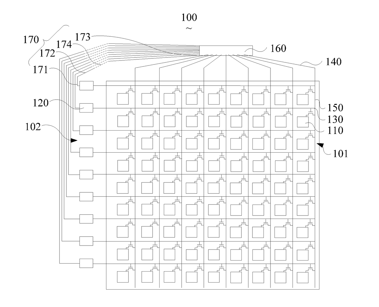
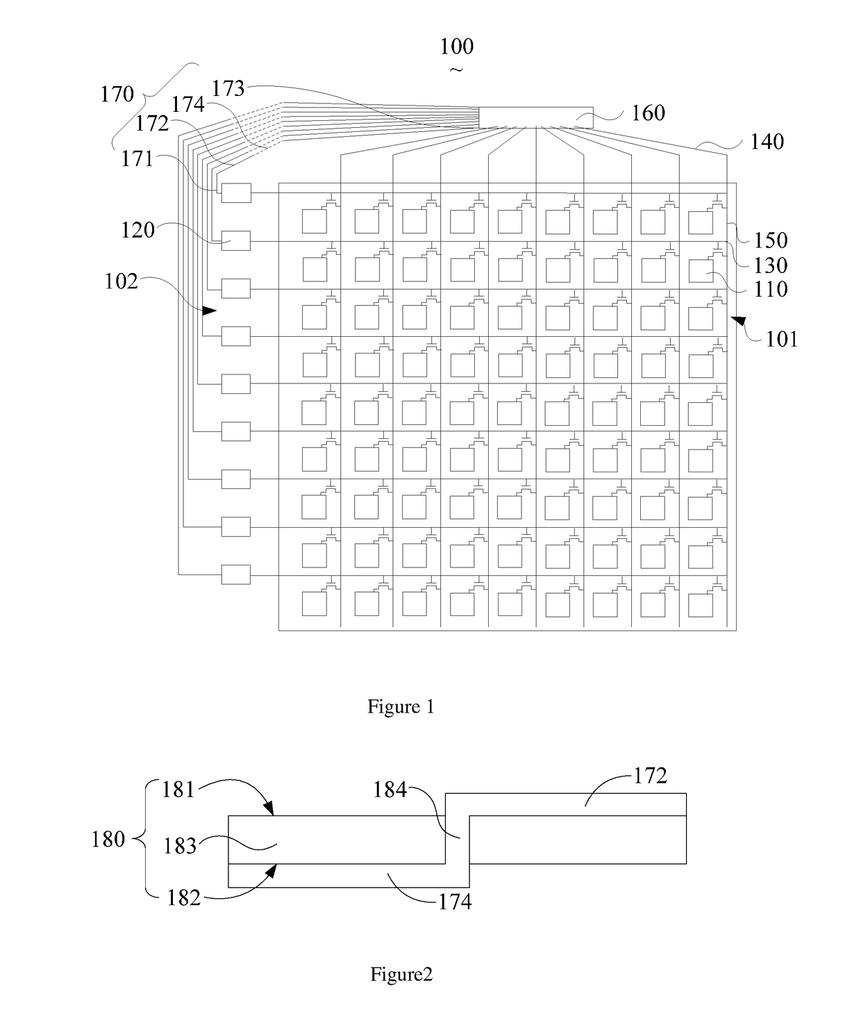
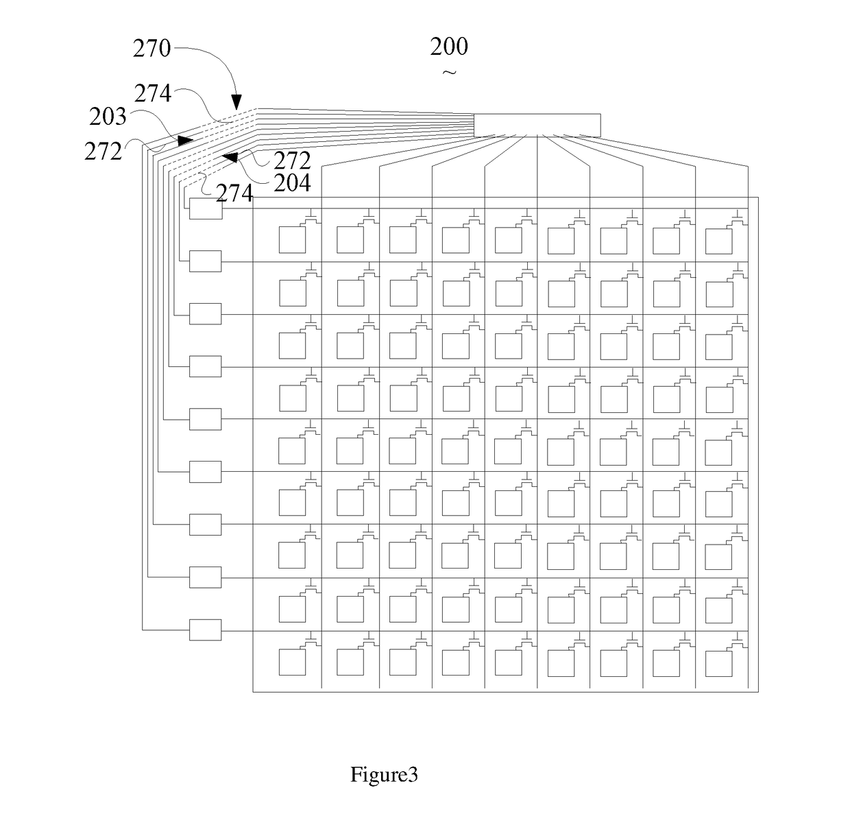
[0046]Referring to FIG. 3, FIG. 3 is a structural illustration of the second embodiment made in accordance to an array substrate in the present invention.

first embodiment

[0047]As shown inFIG. 3, for convenience of explanation, a cross sectional view of a wire on array in different metal layers is illustrated as an example. The structure of the present embodiment is basically the same as that of the the wire on array 270 of array substrate 200 is further divided into a first wire on array region 203 and a second wire on array region 204, wherein a plurality of first wires on array 272 of the first wire on array region 203 and the plurality of first wires on array 272 of the second wire on array region 204 are arranged separately in the same layer. Similarly, a plurality of second wires on array 274 of the first wire on array region 203 and the plurality of second wire on array 274 of the second wire on array region 204 are arranged separately in the same layer.

[0048]Referring to FIG. 4 and FIG. 5, FIG. 4 is a structural illustration of the third embodiment made in accordance to an array substrate in the present invention, FIG. 5 is a cross sectional...


PUM

PropertyMeasurementUnit
distanceaaaaaaaaaa
lengthaaaaaaaaaa
widthaaaaaaaaaa

Abstract

The present invention provides an array substrate, which comprises a display region and a peripheral wiring region, wherein in the peripheral wiring region, gate driving circuits and data driving lines are arranged respectively in correspondence with scanning lines and data lines in the display region and the gate driving circuits are electrically connected to different metal layers arranged in wire on array of the chip on film region to improve the electrostatic protection of the array substrate. Because the array substrate provided by the present invention comprises the wire on array arranged in different metal layers to extend the length of the wire on array and increase the impedance of the wire on array. Thereby the input current of gate driving circuit can be decreased and the probability of gate driving circuit damage can be reduced, the electrostatic protection of the array substrate can be improved.

Description

FIELD OF THE INVENTION[0001]The present invention relates to a technology of display, and more particularly, to a display panel and array substrate thereof.DESCRIPTION OF PRIOR ART[0002]Liquid crystal display (LCD) with a thin body, power saving, no radiation, long life and many other advantages, so it has been widely used. Such as LCD TV, smart phones, digital cameras, computer screens or laptop screens, etc., so that LCD dominates the flat panel display field.[0003]In the case of the usual LCD screen, in order to simplify the design of display panel, the gate driver is arranged inside the glass substrate and the design is called gate on array (GOA) design. In the normal cases, the left and right side or upper side and lower side of GOA is electrically connected by wire on array (WOA) in the GOA design, the WOA is usually used single metal layer wiring. For highly dense and complex GOA circuit, the single metal layer wiring is easy to case the current which is input into the GOA to...

Claims


Application Information

Patent Timeline
Patent Type & Authority Applications(United States)
IPC IPC(8): H01L27/12G02F1/1362G02F1/1345
CPCH01L27/1244G02F1/136204G02F2001/13629G02F1/13454G02F1/136286G02F1/13452H01L27/0248H01L27/124G02F1/13629
Inventor ZHAO, YANG
Owner SHENZHEN CHINA STAR OPTOELECTRONICS TECH CO LTD
Why Eureka
Try Eureka