Eureka AIR delivers breakthrough ideas for toughest innovation challenges, trusted by R&D personnel around the world.

Method of making an electronic device

Inactive Publication Date: 2018-10-18
CAMBRIDGE DISPLAY TECH LTD
View PDF1 Cites 0 Cited by
  • Summary
  • Abstract
  • Description
  • Claims
  • Application Information

AI Technical Summary

Benefits of technology

The present invention provides an electronic device without the need for an unpatterned ITO layer, reducing production costs and complexity.The device has first and second electrically conductive grids that overlap to provide electrical connection between tracks. The busbar is used to conduct a significant electrical current to the grids. The electrically conductive tracks can be made of metal or organic materials, such as nanowires. The material or material composition of the tracks can be chosen based on the properties required for the anode or cathode. The first width of each track is small to improve electronic device performance.

Problems solved by technology

Even though ITO is a suitable material, in particular for lighting devices due to its transparency in the visible spectrum and its high work function, it is relatively expensive mainly due to a limited supply of indium.
The fabrication costs of electronic devices using ITO are further increased as costly vacuum deposition techniques are required for processing ITO.
The device preparation is therefore relatively complex and costly.
Thickness variations in the light emitting layer can result in lower efficiency, reduced lifetime, and non-uniformity in illumination.

Method used


Image

  • Method of making an electronic device
  • Method of making an electronic device
  • Method of making an electronic device

Examples


Embodiment Construction

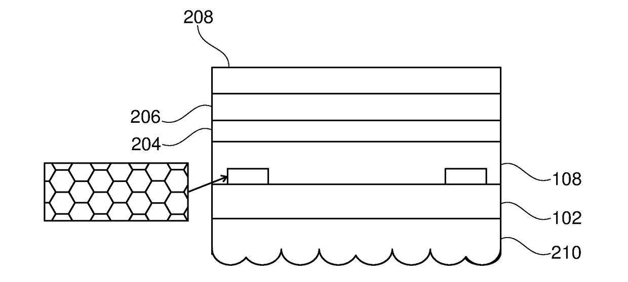
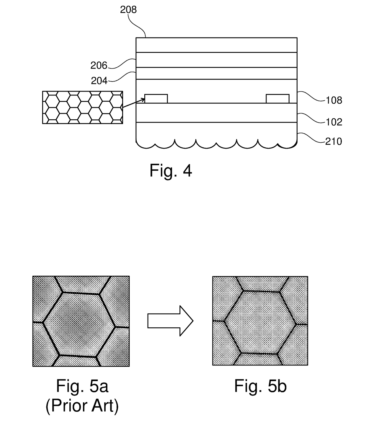
[0079]As outlined above, metal tracking has been exploited in the prior art in order to improve, e.g. the uniformity of light emission over large area tiles.

[0080]Typically, in the prior art, the metal grid and the lateral conductor are prepared in two separate deposition, photo-patterning and etching sequences. This results in high manufacturing costs.

[0081]Furthermore, as outlined above, an additional planarization layer, such as a transparent planarization layer in light-emitting devices, is generally necessary in devices of the prior art which use a single metal grid before deposition of the next active layer (such as hole-injection layer or light emitting layer.

[0082]Embodiments described herein allow for fabricating an electronic device without the need of an additional planarization layer (e.g. a transparent planarization layer in light-emitting devices).

[0083]Furthermore, a separate continuous, unpatterned lateral conductor, such as ITO, can be unecessary in embodiments desc...


PUM


Abstract

A method of fabricating an organic light emitting device comprises patterning a first electrode layer to form a grid comprising a mesh of electrically conductive metal tracks, depositing a layer of hole injection material from a solution comprising less than 10% solids by weight in a solvent, the thickness of the wet layer of solution before the solvent is evaporated to dry the film being greater than the track spacing, evaporating the solvent to provide a dry film having an average thickness in the spacing between the tracks which is less than 10% of the wet thickness of the wet layer of solution and an average thickness in the spacing between the tracks which is greater than 25% of the track thickness to provide a more planar top surface than the surface of the metal tracks before the layer of hole injection material was deposited, depositing one or more further layers from solution to provide a light emitting layer and one or more optional charge transporting layers, and depositing a second electrode layer. The grid can comprise sets of tracks having different widths and spacings.

Description

FIELD OF THE INVENTION[0001]This invention generally relates to a method of making an electronic device, in particular lighting devices, in which an electrode layer of the electronic device comprises first and second electrically conductive grids, and to such an electronic device.BACKGROUND TO THE INVENTION[0002]Recently, metal grids have been exploited in electronic devices to improve device performance. This is particularly the case for large area lighting tiles, where a more uniform light emission may be achieved over the tile as the voltage drop over the anode (or cathode) is distributed more evenly.[0003]For example, in GB 2482110 A, the metal electrode layer is provided as a grid structure. The metal grid may be obtained using standard deposition and patterning / lithography techniques known to those skilled in the art. A separate thin film is used to provide conduction between tracks of the grid.[0004]In order to understand embodiments of the present invention, the following de...

Claims


Application Information

Patent Timeline
IPC IPC(8): H01L51/56H01L51/00
CPCH01L51/56H01L51/0007H01L51/0023H01L51/0028H01L51/5209H01L51/5088H01L51/5012H01L51/5056H01L51/5221H01L51/5268H10K50/17H10K50/813H10K50/81G03F7/0002H10K71/233H10K71/00H10K71/15H10K71/441H10K71/621H10K50/11H10K50/15H10K50/82H10K50/854
Inventor BAKER, COLIN
Owner CAMBRIDGE DISPLAY TECH LTD
Why Eureka
Eureka Blog
Learn More