Process for producing an array of mesa-structured photodiodes

Active Publication Date: 2018-10-25
COMMISSARIAT A LENERGIE ATOMIQUE ET AUX ENERGIES ALTERNATIVES
View PDF0 Cites 5 Cited by
  • Summary
  • Abstract
  • Description
  • Claims
  • Application Information

AI Technical Summary

Benefits of technology

[0030]The thickness of the passivation layer, at the lateral surface

Problems solved by technology

However, this process envisages the use of multiple etch or deposition masks, and hence multiple steps of structuring the masks by means of photolithography, which may result in a lack of accuracy in the positioning of the diode contacts 11 and of the passivation layer 14 with respect to the mesa structures 2.
This lack of accuracy in positioning may be particularly restrictive

Method used


Image

  • Process for producing an array of mesa-structured photodiodes
  • Process for producing an array of mesa-structured photodiodes
  • Process for producing an array of mesa-structured photodiodes

Examples


Embodiment Construction

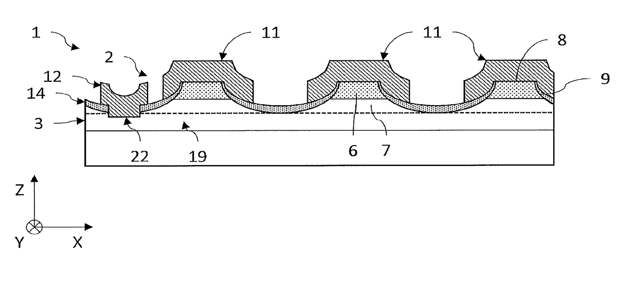
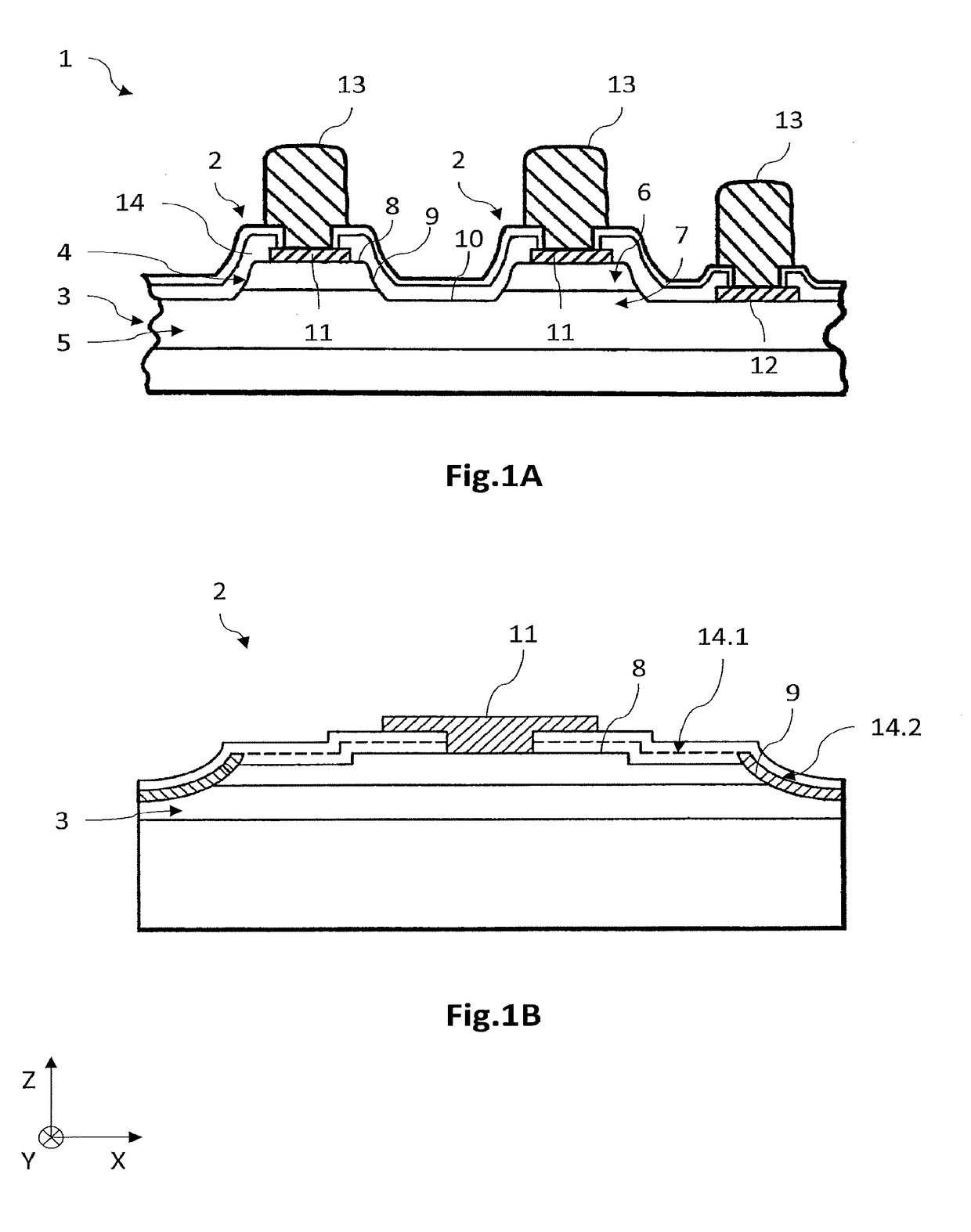
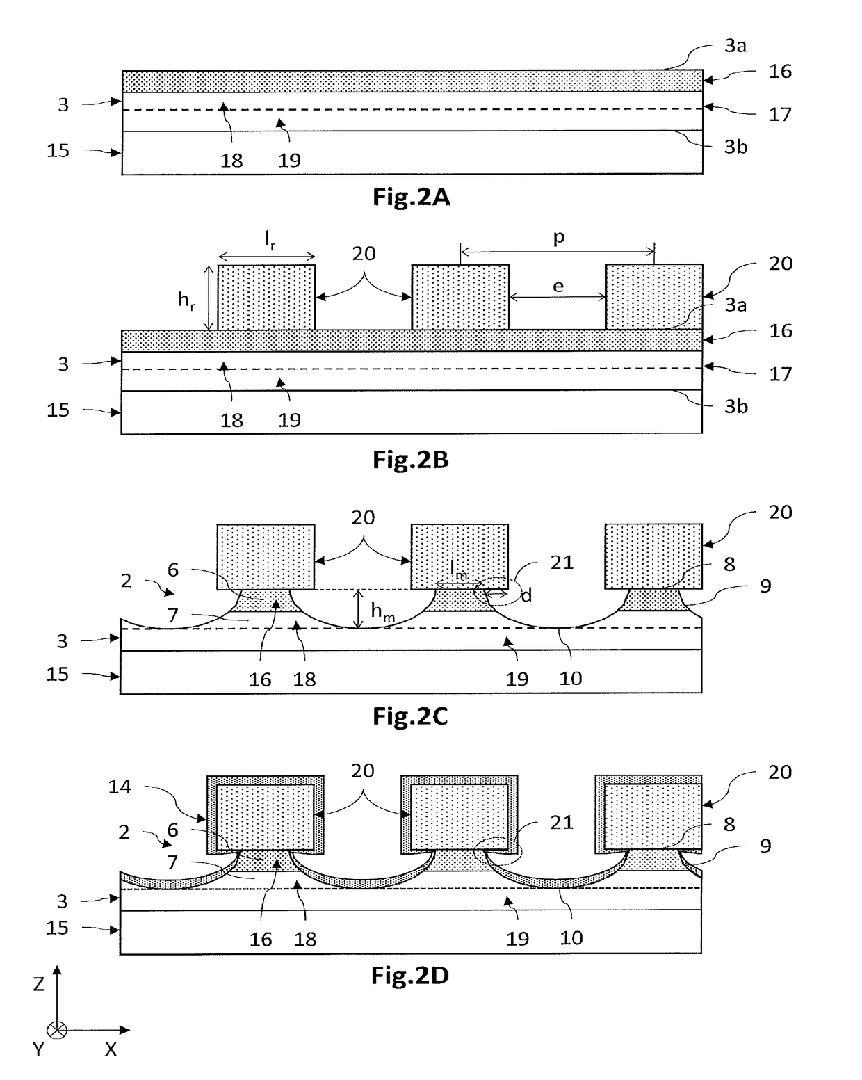
[0038]In the figures and in the subsequent description, the same references represent identical or similar elements. Moreover, the various elements are not represented to scale so as to enhance the clarity of the figures. Furthermore, the various embodiments and variants are not mutually exclusive and may be combined with one another. Unless indicated otherwise, the terms “substantially”, “about” and “of the order of” mean to within 10%.

[0039]FIGS. 2A to 2H illustrate various steps of a process for producing an array of mesa-structured photodiodes according to one example of an embodiment. In this example, the useful layer is made of an alloy of cadmium, mercury and tellurium, in this instance CdHgTe, obtained by epitaxial growth from a growth substrate, referred to hereinafter as the carrier layer. The term “useful layer” is understood to mean a layer made of at least one semiconductor material, at least part of which is capable of absorbing the electromagnetic radiation to be dete...


PUM


Abstract

The invention pertains to a process for producing an array (1) of mesa-structured photodiodes (2), including at least the following steps:
a) producing a useful layer (3);
b) producing an etch mask formed of a plurality of etch pads (20);
c) wet-etching part of the useful layer (3) located between the etch pads (20), forming a plurality of mesa-structured photodiodes (2), producing a recess (21);
d) conformally depositing a passivation layer (14);
e) removing the etch pads (20) by chemical dissolution;
f) producing conductive pads (11).

Description

TECHNICAL FIELD[0001]The field of the invention is that of mesa-structured photodiodes, used in particular for detecting infrared radiation.STATE OF THE PRIOR ART[0002]FIG. 1A illustrates one example of an array 1 of mesa-structured photodiodes 2 made of CdHgTe such as described in document U.S. Pat. No. 5,401,986. Each photodiode 2 is structured like a mesa, that is to say it is formed of an upper part 4 of a layer, referred to as the useful layer 3, made of CdHgTe, this upper part 4 protruding with respect to a lower part 5 of the useful layer 3, referred to as the base, extending below the photodiodes 2. Each upper part 4 includes a first portion 6, which is here p-doped, covering a second portion 7, which is here n-doped, so as to form a p-n junction. Each mesa structure 2, i.e. the part 4 protruding with respect to the base 5, has its own p-n junction, thus forming a photodiode 2.[0003]Each photodiode 2 includes an upper surface 8, the border of which is delimited by lateral su...

Claims


Application Information

Patent Timeline
IPC IPC(8): H01L31/18H01L27/144H01L31/02H01L31/103H01L31/0352
CPCH01L31/1828H01L27/1443H01L31/02002H01L31/1032H01L31/035281H01L31/02966H01L31/102H01L31/1832H01L31/1868Y02P70/50H01L27/144H01L31/02H01L31/0352Y02E10/50
Inventor BADANO, GIACOMOLOBRE, CLEMENTESPIAU DE LAMAESTRE, ROCHCHAMONAL, JEAN-PAUL
Owner COMMISSARIAT A LENERGIE ATOMIQUE ET AUX ENERGIES ALTERNATIVES
Why Eureka
Try Eureka