Nano-featured porous silicon materials

a porous silicon and nano-feature technology, applied in silicon compounds, cell components, electrochemical generators, etc., can solve the problems of low power performance and limited capacity of graphitic anodes, insufficient current lead acid automobile batteries for next-generation all-electric and hybrid electric vehicles, and fundamental limitations of materials, etc., to achieve high first cycle efficiency, optimize lithium storage and utilization properties, and high reversible capacity

Active Publication Date: 2018-11-15
GRP 14 TECH INC
View PDF0 Cites 36 Cited by
  • Summary
  • Abstract
  • Description
  • Claims
  • Application Information

AI Technical Summary

Benefits of technology

[0005]In general terms, the current invention is directed to porous silicon materials, and their manufacturing, and composites comprising the porous silicon materials and hard carbon materials, and their manufacturing. The porous silicon materials and the composites that contain the porous silicon materials and hard carbon materials provide optimized lithium storage and utilization properties. The novel porous silicon and composite materials find utility in any number of electrical energy storage devices, for example as electrode material in lithium-based electrical energy s

Problems solved by technology

For example, current lead acid automobile batteries are not adequate for next generation all-electric and hybrid electric vehicles due to irreversible, stable sulfate formations during discharge.
Traditional lithium ion batteries are comprised of a graphitic carbon anode and a metal oxide cathode; however such graphitic anodes typically suffer from low power performance and limited capacity.
However, these materials are fundamentally limited by the substantial swelling that occurs when they are fully lithiated.
This swelling and shrinkage when the lithium is removed result

Method used


Image

  • Nano-featured porous silicon materials
  • Nano-featured porous silicon materials
  • Nano-featured porous silicon materials

Examples


example 1

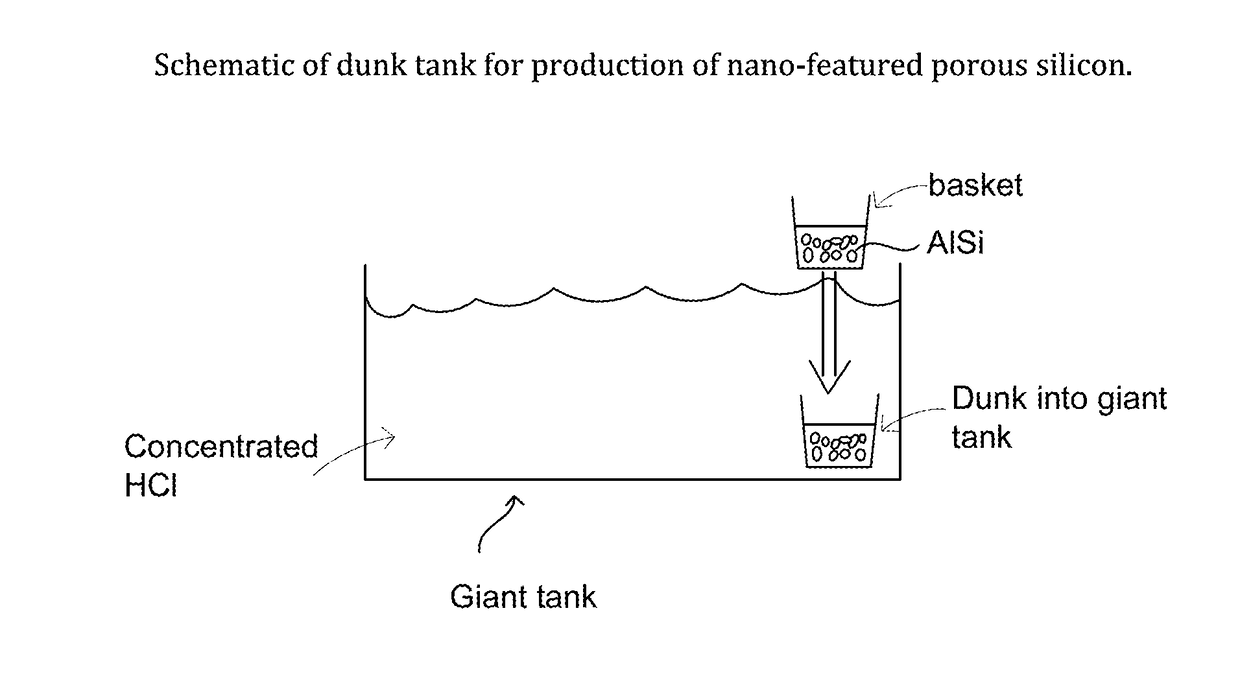
Etching of Al—Si Alloy to Yield Bulk Porous Silicon

[0186]Aluminum-silicon alloy was dispersed in water and mixed by overhead mixer. Hydrochloric acid was added the dispersion over time, generating heat and accomplishing the etching. To avoid boiling, the heat generated is removed from the reactor by adding water ice to the system. Other modes to remove heat, such as employing a heat exchanger of varying modes of other approaches can also be employed, as known in the art. After the etching reaction subsided, the solids were allowed to settle in the reaction tank, and excess water decanted. The wet cake was dried in an oven, for example at 130 C, to yield dried, porous silicon with nano-scaled features. Alternatively, additional drying at a higher temperature, for example 450 C under an inert environment such as nitrogen gas, is also employed to yield the final dried, porous silicon. Alternatively, additional drying at a higher temperature, for example 1050 C under an inert environmen...

example 2

Particle Size Reduction of Bulk Porous Silicon

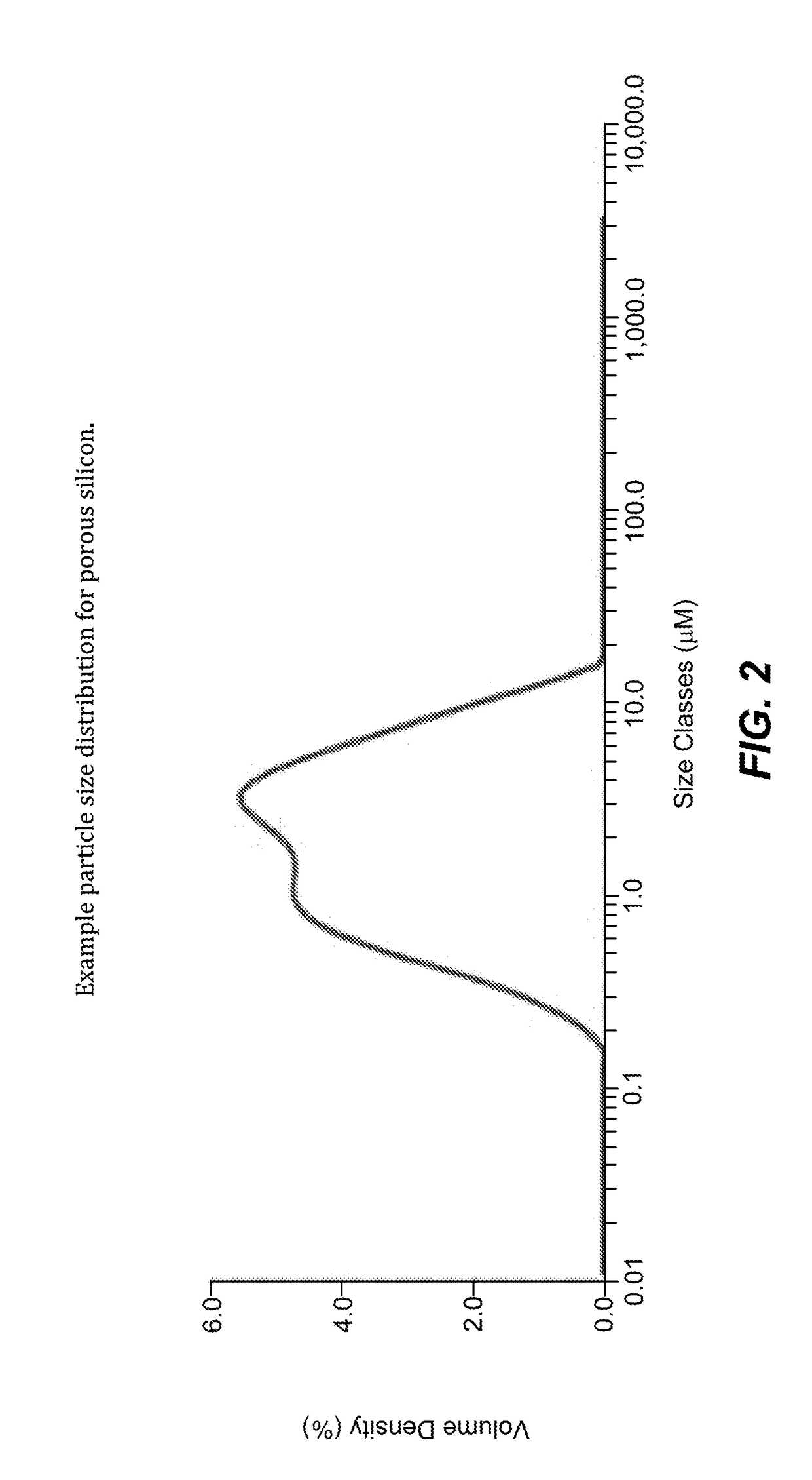
[0188]The bulk porous silicon from Example 1 can be size reduced, for example by methods known in the art such as grinding, ball milling, jet milling, water jet milling, and other approaches known in the art. In one embodiment, the porous silicon is particle sized reduced by jet milling. Example particle size distributions before and after jet milling are shown in FIG. 2 and FIG. 3, respectively. Before jet milling, the measured Dv0, Dv1, Dv5, Dv10, Dv20, Dv50, Dv80, Dv890, Dv95, Dv100 were 167 nm, 250 nm, 384 nm, 506 nm, 742 nm, 1.96 um, 4.63 um, 6.64 um, 12.0 um, and 16.2 um, respectively. This material was predominantly micron-sized, for example the Dv50 was 1.96 microns. After jet milling, the measured Dv0, Dv1, Dv5, Dv10, Dv20, Dv50, Dv80, Dv90, Dv99, and Dv100 were 146 nm, 194 nm, 290 nm, 388 nm, 505 nm, 766 nm, 1.10 um, 1.28 um, 1.65 um, and 1.87 um, respectively.

[0189]As can be seen, the porous silicon described herein was suffic...

example 3

Particle Size Reduction of Non-Porous Silicon

[0190]Employing the same jet milling strategy as for Example 2, an attempt was conducted to particle size reduce a commercially available non-porous silicon. Example particle size distributions before and after jet milling are shown in FIG. 4 and FIG. 5, respectively. Before jet milling, the measured Dv0, Dv1, Dv5, Dv10, Dv20, Dv50, Dv80, Dv890, Dv95, Dv100 were 147 nm, 247 nm, 546 nm, 702 nm, 942 nm, 1.66 um, 3.03 um, 4.64 um, 17.1 um, and 23.9 um, respectively. This material was predominantly micron-sized, for example the Dv50 was 1.66 microns. After jet milling, the measured Dv0, Dv1, Dv5, Dv10, Dv20, Dv50, Dv80, Dv90, Dv99, and Dv100 were 147 nm, 245 nm, 525 nm, 685 nm, 924 nm, 1.62 nm, 2.79 um, 3.79 um, 12.5 um, and 18.6 um, respectively. As can be seen, the non-porous silicon was non-friable. There was no appreciable particle size reduction upon jet milling the jet milled non-porous silicon remained micron-sized, specifically, the D...


PUM

PropertyMeasurementUnit
Temperatureaaaaaaaaaa
Fractionaaaaaaaaaa

Abstract

Porous silicon and methods for preparation and use of the same are disclosed. The porous silicon materials have utility either alone or in combination with other materials, for example, combined with carbon particles for energy storage applications.

Description

BACKGROUNDTechnical Field[0001]The present invention generally relates to porous silicon materials, and carbon-impregnated silicon materials produced therefrom, and related manufacturing methods. The silicon materials exhibit nano-features and extraordinary friability. The porous silicon materials and / or carbon-impregnated silicon materials have utility either alone or in combination with other materials, for example, combined with carbon particles as composition of matter for energy storage applications. Said energy storage applications include employing the materials herein as electrode materials for lithium ion batteries and related energy storage devices employing lithium or lithium ions, for instance lithium air batteries. In certain embodiments, the materials disclosed herein have utility as anode materials for energy storage devices such as lithium ion batteries and related energy storage device employing lithium or lithium ions. Thus, the present invention also relates to co...

Claims


Application Information

Patent Timeline
IPC IPC(8): H01M4/38C01B33/021H01M10/0525C09K23/54
CPCH01M4/386C01B33/021H01M10/0525C01P2006/40C01P2006/10C01P2006/12C01P2006/14C01P2006/17C01P2006/80C01P2004/03C01P2002/72C01P2002/85H01M2004/021H01M2004/027C23F1/00C01P2006/16C01P2006/21Y02E60/10Y02E60/50H01M8/1037C01P2006/11H01M4/366H01M4/587
Inventor FEAVER, AARON M.THOMPKINS, LEAH A.GERAMITA, KATHARINEKRON, BENJAMIN E.SAKSHAUG, AVERY J.FREDRICK, SARAHCOSTANTINO, HENRY R.GOODWIN, CHADTIMMONS, CHRISTOPHER
Owner GRP 14 TECH INC
Why Eureka
Try Eureka