Electro-optical device and electronic apparatus
a technology of optical devices and electronic devices, applied in the direction of semiconductor devices, optics, instruments, etc., can solve the problems of unstable operation of cracks in insulating films, and failure to operate sample and hold circuits properly, etc., to achieve stable operation and high reliability quality
- Summary
- Abstract
- Description
- Claims
- Application Information
AI Technical Summary
Benefits of technology
Problems solved by technology
Method used
Image
Examples
first embodiment
[0065]Electro-Optical Device
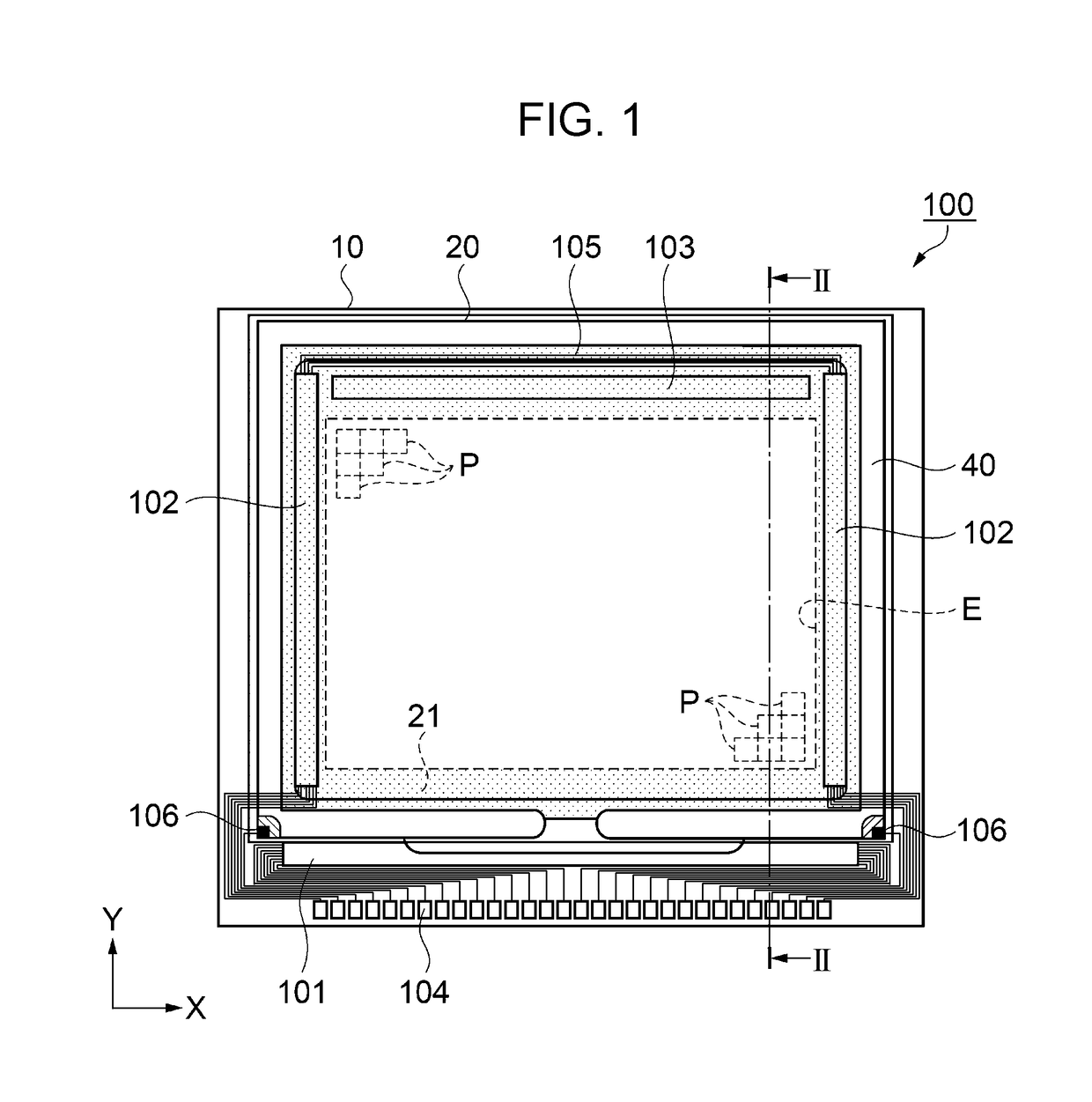
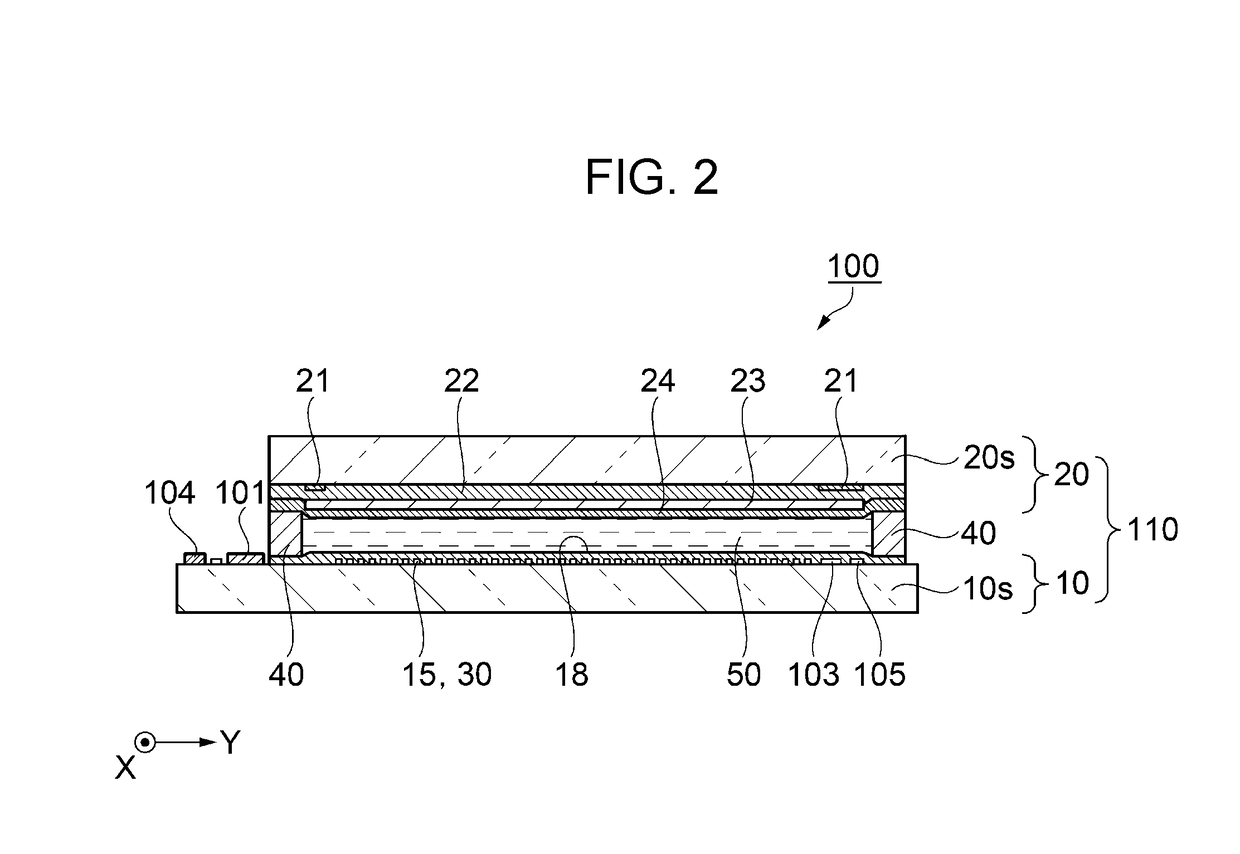
[0066]First, a schematic configuration of a liquid crystal device as an electro-optical device of this embodiment will be described with reference to FIGS. 1 and 2. FIG. 1 is a schematic plan view showing a configuration of a liquid crystal device, and FIG. 2 is a schematic sectional view taken along the line II-II of the liquid crystal device shown in FIG. 1.
[0067]As shown in FIGS. 1 and 2, a liquid crystal device 100 as an electro-optical device of this embodiment includes an element substrate 10 and an opposing substrate 20 that are disposed opposite to each other, and a liquid crystal layer 50 sandwiched between the pair of substrates. For the base material 10s of the element substrate 10 and the base material 20s of the opposite substrate 20, for example, a transparent quartz substrate or a glass substrate are used.
[0068]The element substrate 10 is slightly larger than the opposite substrate 20, both substrates are adhered via a sealing material 40 d...
modification example 1
[0146]As shown in FIG. 14, the sample and hold (SH) circuit 7 of Modification Example 1 includes the sampling transistors (S-TFT) 71 made of a plurality of (four) transistors 71A, 71B, 71C, and 71D aligned in the Y direction in which a linear gate line 71g extends, and connected in parallel. Under the layer of the plurality of transistors 71A, 71B, 71C, and 71D, a light shielding layer 76 divided for each of the plurality of transistors 71A, 71B, 71C, and 71D in the Y direction is provided. The channel widths in the plurality of transistors 71A, 71B, 71C, and 71D and the width L4 of the divided light shielding layer 76 in the Y direction are about 150 μm as described above. The SH circuit 7 and the light shielding layer 76 are provided on the element substrate 10.
[0147]As shown in FIG. 15, the light shielding layer 76 is divided in a state of straddling three transistors in the X direction. The light shielding layer 76 is divided such that the division position of the light shieldin...
modification example 2
[0153]As shown in FIG. 18, the sample and hold (SH) circuit 7 of Modification Example 2 includes the sampling transistors (S-TFT) 71 made of a plurality of (four) transistors 71A, 71B, 71C, and 71D aligned in the Y direction in which a linear gate line 71g extends and connected in parallel. Under the layer of a plurality of transistors 71A, 71B, 71C, and 71D, a light shielding layer 77 divided for each of the plurality of transistors 71A, 71B, 71C, and 71D in the Y direction is provided. The channel widths in the plurality of transistors 71A, 71B, 71C and 71D, and the width L4 of the divided light shielding layer 77 in the Y direction are about 150 μm as described above. The SH circuit 7 and the light shielding layer 77 are provided on the element substrate 10.
[0154]The light shielding layer 77 is disposed so as to overlap two transistors (the semiconductor layer 70a) adjacent in the X direction, and has portions that protrude in the X direction, corresponding to the source contact ...
PUM
| Property | Measurement | Unit |
|---|---|---|
| length | aaaaa | aaaaa |
| length | aaaaa | aaaaa |
| width | aaaaa | aaaaa |
Abstract
Description
Claims
Application Information


