Multi-Nyquist Zone Digital-to-Analog Converter (DAC)

a digital-to-analog converter and multi-nyquist technology, applied in the field of digital-to-analog converters (dacs), can solve the problems of not being well suited to integration with digital logic, signal bandwidth and linearity remain a big challenge, and achieve a wide signal bandwidth

Active Publication Date: 2019-01-10
AMERICAN RES CAPITAL LLC
View PDF0 Cites 2 Cited by
  • Summary
  • Abstract
  • Description
  • Claims
  • Application Information

AI Technical Summary

Problems solved by technology

While the availability of such heterojunction bipolar transistor (HBT) devices helps with the signal bandwidth, these technologies are not well suited for integration with digital logic.
It has been shown [2] that the most advanced CMOS nodes are suitable for designing DACs with record braking update rates, but signal bandwidth and linearity remain a big challenge.
It can be argued that achieving a wide signal bandwidth is an even bigger challenge in very high speed DAC design than is realizing a faster update rate.
Thus, even if sampled at a rate high enough to satisfy the Nyquist criteria, the use of conventional CMOS circuitry limits a CMOS ADC to output frequencies of less than 20 GHz.
However, the use of buffers would contribute noise, distortion, and significant power usage, while only pushing the problem to the input of the buffer.
However, the problem would remain in the via stack used to transition between IC metal stacks (typically 10 or more) to access the S / D.
Since a large percentage of the DAC functions are performed in the digital domain, it would be undesirable to design an IC with via thicknesses sufficient to support high frequency analog signals.
However, using thicker metals and SiGe transistors to enable collocated logic circuitry would make for large, power demanding ICs at an impractical price.

Method used


Image

  • Multi-Nyquist Zone Digital-to-Analog Converter (DAC)
  • Multi-Nyquist Zone Digital-to-Analog Converter (DAC)
  • Multi-Nyquist Zone Digital-to-Analog Converter (DAC)

Examples


Embodiment Construction

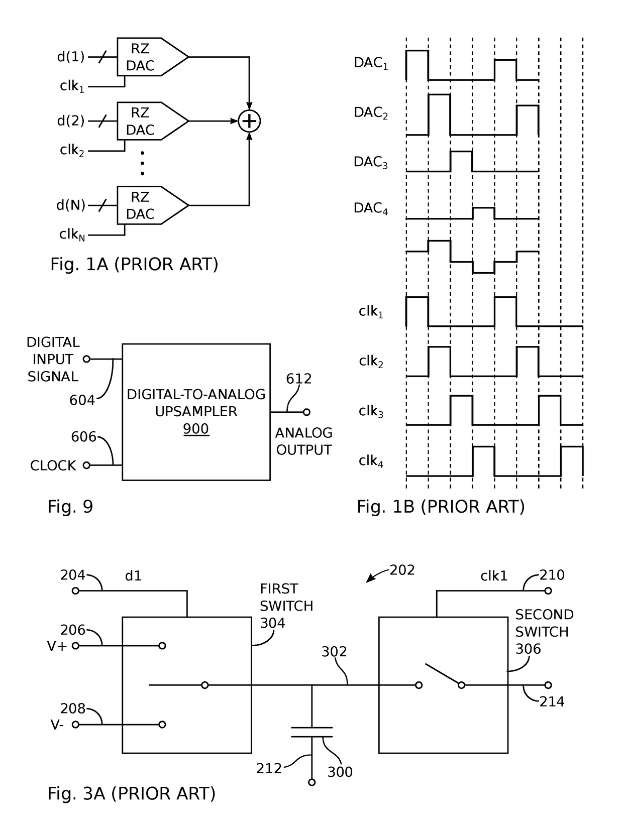
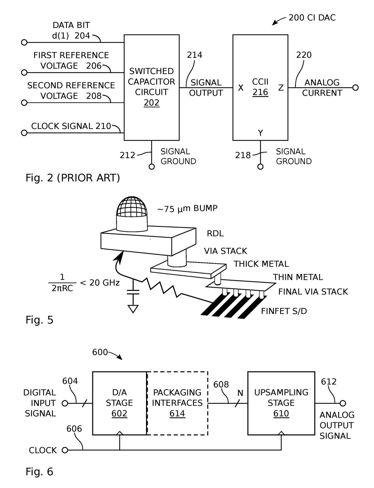
[0052]FIG. 6 is a schematic block diagram of an exemplary multi-zone digital-to-analog device. The multi-zone device 600 comprises a digital-to-analog (D / A) stage 602 having an input on line 604 to accept a digital input signal with a data bandwidth of M Hertz (Hz). A clock input on line 606 accepts a clock signal with a clock frequency of P Hz, and an output on line 608 supplies an analog value having a bandwidth of M Hz. An upsampling stage 610 having an input on line 608 to accept the analog value and a clock input on line 606 accepts the clock signal. The upsampling stage 610 has a device bandwidth of L Hz, meaning that essential active devices have the ability to operate with a bandwidth of L Hz regardless of the bandwidth of the analog output signals actually supplied. The upsampling stage 610 supplies an analog output signal with a full power bandwidth of K Hz on line 612, where (P / 2)=M and M602 supplies N deinterleaved analog values on line 608 having a combined bandwidth of...


PUM


Abstract

A multi-zone digital-to-analog device is provided with a digital-to-analog (D / A) stage having an input to accept a digital input signal with a data bandwidth of M Hertz (Hz), a clock input to accept a clock signal with a clock frequency of P Hz, and an output to supply an analog value having a bandwidth of M Hz. An upsampling stage has an input to accept the analog value and a clock input to accept the clock signal. The upsampling stage has a device bandwidth of L Hz to supply an analog output signal with a full power bandwidth of K Hz, where (P / 2)=M and M<K<L. The upsampling stage supplies analog output signal images in a plurality of Nyquist zones. In one aspect, the D / A stage supplies N deinterleaved analog values having a combined bandwidth of M Hz, where N×(P / 2)=M.

Description

RELATED APPLICATIONS[0001]Any and all applications, if any, for which a foreign or domestic priority claim is identified in the Application Data Sheet of the present application are hereby incorporated by reference under 37 CFR 1.57.[0002]The following applications are also incorporated herein by reference:[0003]N-PATH INTERLEAVING ANALOG-TO-DIGITAL CONVERTER (ADC) WITH BACKGROUND CALIBRATION, invented by Mikko Waltari, Ser. No. 14 / 531,371, filed Nov. 3, 2014, now U.S. Pat. No. 9,030,340;[0004]INTERLEAVING ANALOG-TO-DIGITAL CONVERTER (ADC) WITH BACKGROUND CALIBRATION, invented by Mikko Waltari et al., Ser. No. 14 / 511,206, filed Oct. 10, 2014, now U.S. Pat. No. 8,917,125;[0005]TIME-INTERLEAVED ANALOG-TO-DIGITAL CONVERTER FOR SIGNALS IN ANY NYQUIST ZONE, invented by Mikko Waltari, Ser. No. 13 / 603,495, filed Sep. 5, 2012, issued as U.S. Pat. No. 8,654,000 on Feb. 18, 2014.[0006]CURRENT IMPULSE (CI) DIGITAL-TO-ANALOG CONVERTER (DAC), invented by Mikko Waltari, Ser. No. 14 / 750,203, filed...

Claims


Application Information

Patent Timeline
Patent Type & Authority Applications(United States)
IPC IPC(8): H03M1/66H04B1/44
CPCH04B1/44G11C27/02H03L7/08H03M1/662H03L7/0812H03M1/06H03M1/121
Inventor KAPPES, MICHAELNORSWORTHY, STEVEN R.PALA, COSTANTINO
Owner AMERICAN RES CAPITAL LLC
Why Eureka
Try Eureka