Methods of Transferring a Graphene Monolayer via a Stacked Structure and Devices Fabricated Thereby

a technology of stacked structure and transfer method, which is applied in the direction of semiconductor devices, basic electric elements, electrical equipment, etc., can solve the problems of affecting the electronic response of graphene, and affecting the synthesis process

Inactive Publication Date: 2019-02-14
THE UNITED STATES OF AMERICA AS REPRESENTED BY THE SECRETARY OF THE NAVY
View PDF6 Cites 2 Cited by
  • Summary
  • Abstract
  • Description
  • Claims
  • Application Information

AI Technical Summary

Problems solved by technology

However, due to an atomic thickness of only a single atom, traditional fabrication processes fail.
The result is degradation of the electronic response of graphene.
However, the temperatures required for proper graphene synthesis tend to damage die substrates.

Method used


Image

  • Methods of Transferring a Graphene Monolayer via a Stacked Structure and Devices Fabricated Thereby
  • Methods of Transferring a Graphene Monolayer via a Stacked Structure and Devices Fabricated Thereby
  • Methods of Transferring a Graphene Monolayer via a Stacked Structure and Devices Fabricated Thereby

Examples


Embodiment Construction

)

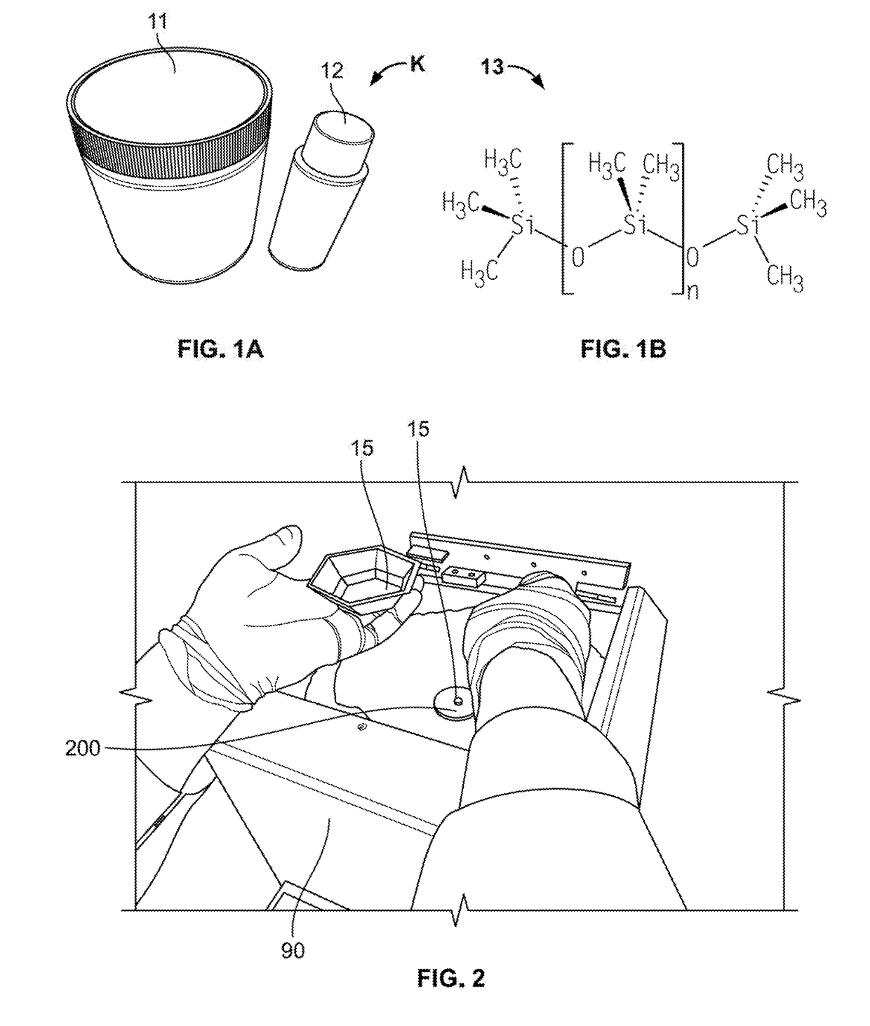
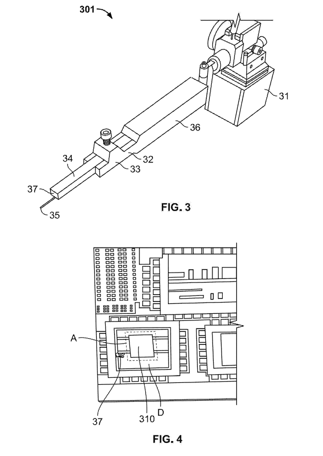
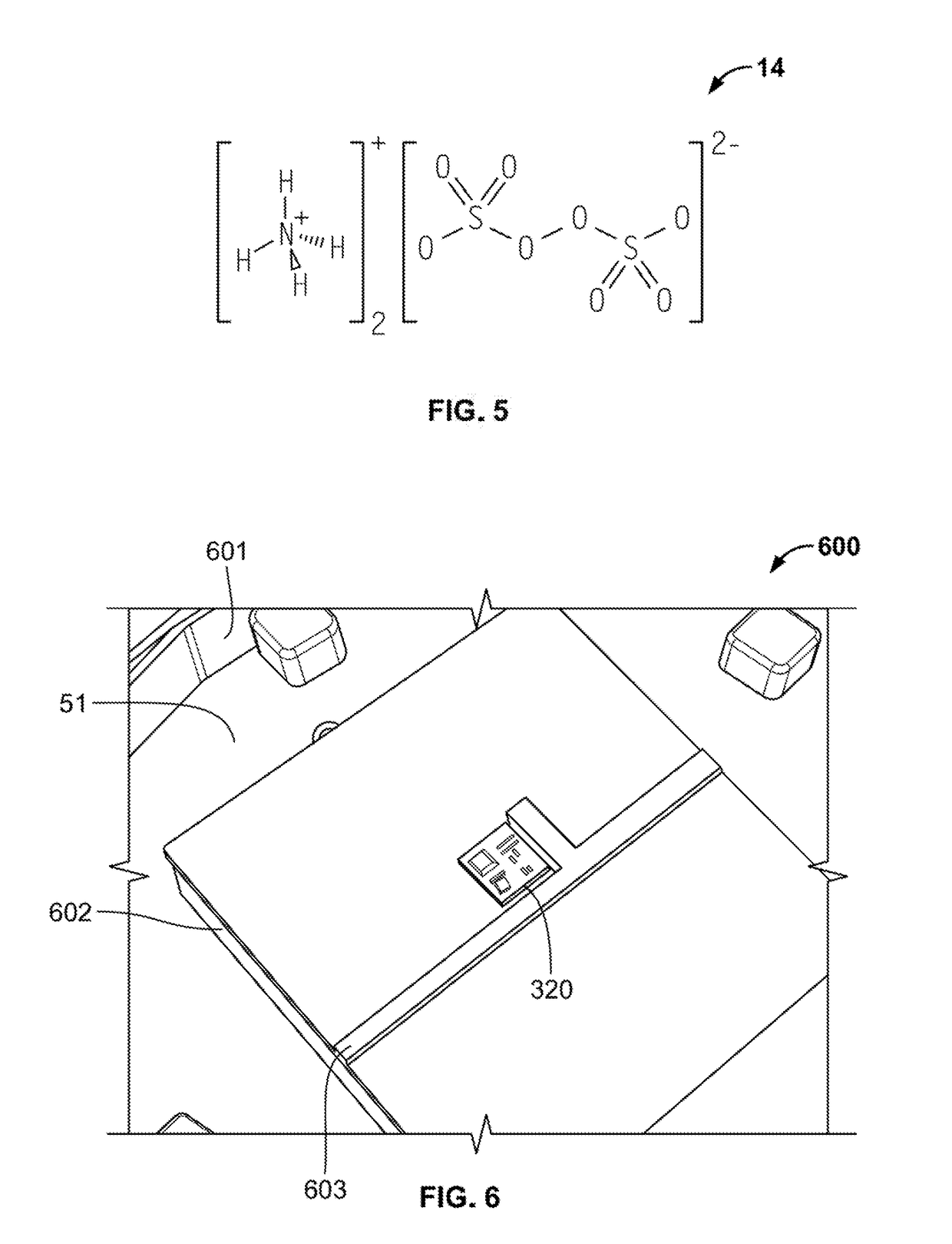
[0018]The present disclosure encompasses a method of preparing and transferring a graphene monolayer onto a stacked structure, wherein the graphene monolayer comprises a single layer of carbon atoms responsive to the presence of adsorbates for facilitating sensing thereof. The graphene monolayer has linear energy dispersion and two-dimensional structure properties which facilitate its use in nanoscale applications and in atomic level charge particle detection via charge detection on a surface of the graphene monolayer. In accordance with some embodiments of present disclosure, the method of preparing and transferring a graphene monolayer onto a stacked structure alternatively involves using an additive manufacturing technique, such as using a 3D printed platform. Graphene is synthesized on a metal catalyst layer, such as at least one of copper (e.g., a copper film), boron nitride, and nickel, by way of a chemical vapor deposition (CVD) from a carbon source. The embodiments of the p...


PUM

PropertyMeasurementUnit
temperatureaaaaaaaaaa
thicknessaaaaaaaaaa

Abstract

A method of fabricating a graphene device generally involving depositing a graphene monolayer from a carbon source on a metal catalyst layer; depositing a transfer substrate on the graphene monolayer by way of casting, thereby forming a transfer-substrate/graphene/metal-catalyst structure; annealing the transfer-substrate/graphene/metal-catalyst structure, thereby forming an annealed transfer-substrate/graphene/metal-catalyst structure; coupling a thermal adhesive with the transfer-substrate/graphene/metal-catalyst structure; moving the annealed transfer-substrate/graphene/metal-catalyst structure to a target area of a target device, by using a probe assembly or the like, thereby forming an annealed transfer-substrate/graphene/metal-catalyst/thermal-adhesive/target-device structure; releasing the slip of thermal adhesive from the annealed transfer-substrate/graphene/metal-catalyst thermal-adhesive/target-device structure by applying heat, thereby forming an annealed transfer-substrate/graphene/metal-catalyst/target-device structure; etching away the metal catalyst layer from the annealed transfer-substrate/graphene/metal-catalyst/target-device structure in an etching solution, thereby forming a graphene/transfer-substrate/target-device structure; rinsing the graphene/transfer-substrate/target-device structure with DI water, thereby removing any excess etching solution; and drying the graphene/transfer-substrate/target-device structure, thereby providing the graphene device.

Description

FEDERALLY-SPONSORED RESEARCH AND DEVELOPMENT[0001]The United States Government has ownership rights in the subject matter of the present disclosure. Licensing inquiries may be directed to Office of Research and Technical Applications, Space and Naval Warfare Systems Center, Pacific, Code 72120, San Diego, Calif., 92152; telephone (619) 553-5118; email: ssc_pac_t2@navy.mil. Reference Navy Case No. 102,799.BACKGROUND OF THE INVENTIONTechnical Field[0002]The present disclosure technically relates to graphene structures. Particularly, the present disclosure technically relates to fabrication of graphene structures.Description of Related Art[0003]In the related art, graphene is a two-dimensional layer of carbon atoms arranged in a honeycomb crystal lattice held together by strong Van der Waals forces. Graphene research has shown enormous potential in the areas of device physics and clean energy. However, due to an atomic thickness of only a single atom, traditional fabrication processes ...

Claims


Application Information

Patent Timeline
Patent Type & Authority Applications(United States)
IPC IPC(8): H01L21/683H01L21/02H01L21/78
CPCH01L21/6836H01L21/02527H01L21/02425H01L21/0262H01L21/7806H01L21/02079H01L21/02118H01L21/02282H01L2221/68318H01L2221/68363H01L2221/68381H01L31/1804H01L31/1892H01L29/1606
Inventor KAMIN, NACKIEB M.DE ANDRADE, MARCIO C.GARMIRE, DAVIDORDONEZ, RICHARD C.
Owner THE UNITED STATES OF AMERICA AS REPRESENTED BY THE SECRETARY OF THE NAVY
Why Eureka
Try Eureka