Method and System for Forming a Multilayer Composite Structure

a composite structure and multi-layer technology, applied in the direction of reducing the size of cables/conductors, conductingors, single bars/rods/wires/strips, etc., can solve the problem that the effective conductivity of nanowires is usually not significantly larger, and achieves a high volume percentage of graphene. , the effect of efficient mass production

Active Publication Date: 2019-02-28
ULTRA CONDUCTIVE COPPER CO INC
View PDF9 Cites 8 Cited by
  • Summary
  • Abstract
  • Description
  • Claims
  • Application Information

AI Technical Summary

Benefits of technology

[0004]In view of the known prior art, what is needed is an improved method for forming a multilayer composite stru...

Problems solved by technology

However, the effective conductivity of these nanowires is usually not significantly ...

Method used


Image

  • Method and System for Forming a Multilayer Composite Structure
  • Method and System for Forming a Multilayer Composite Structure
  • Method and System for Forming a Multilayer Composite Structure

Examples


Embodiment Construction

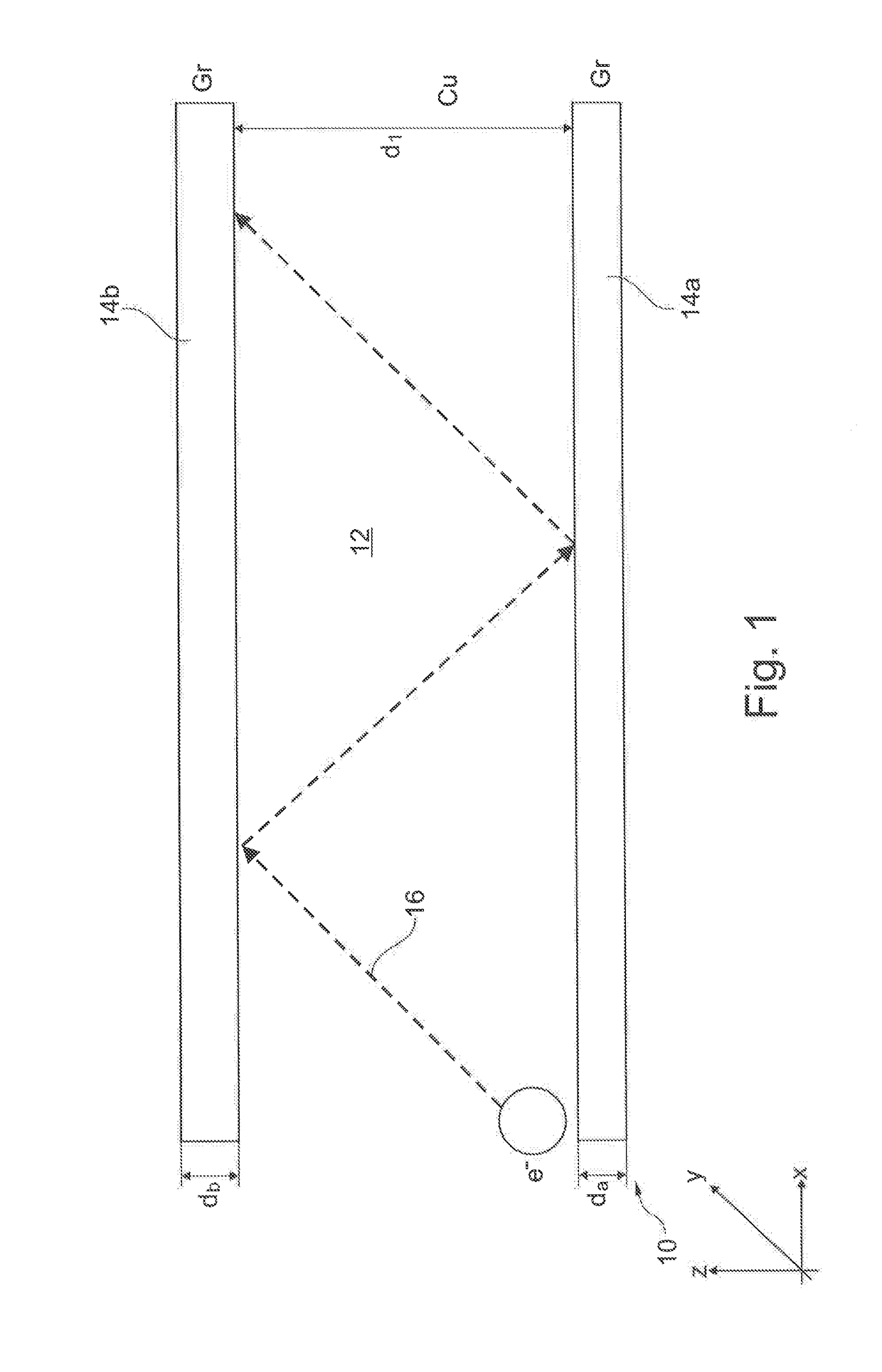
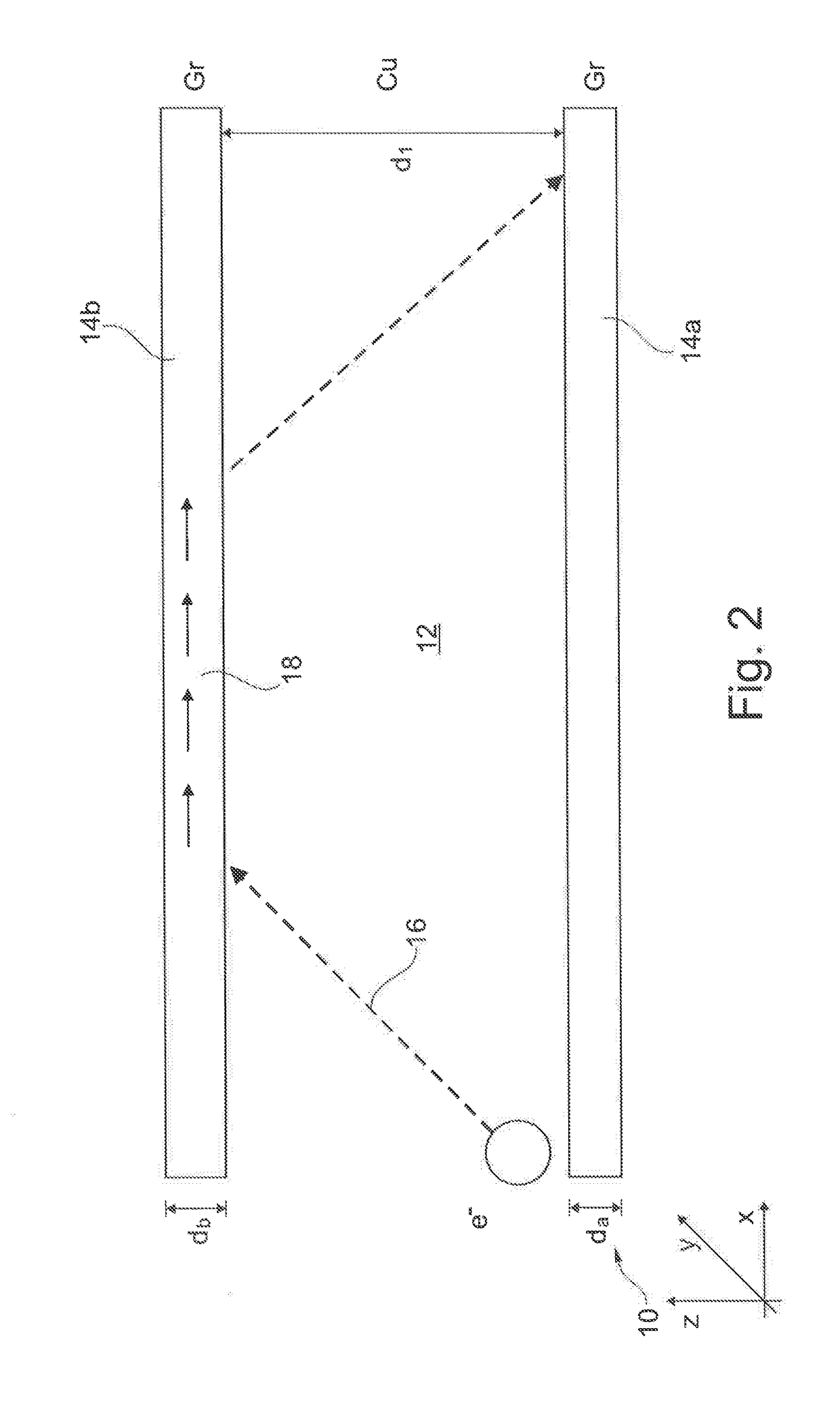
[0151]FIG. 1 is a schematic illustration of the composite structure 10 according to an example in a cross-sectional view. The composite structure 10 comprises a copper layer 12 sandwiched by a first (lower) graphene layer 14a and a second (upper) graphene layer 14b.

[0152]The copper layer 12 may be formed of pure copper (Cu), in particular in a (111) crystallographic orientation. However, in other examples, the copper layer comprises additional material other than copper, such as doped atoms or nanoparticles, as will be described in more detail below.

[0153]The copper layer 12 as shown in FIG. 1 extends at a width or thickness d1 between the first graphene layer 14a and the second graphene layer 14b, wherein d1 is generally no larger than 25 μm. For instance, the copper layer 12 may be formed at a thickness of 20 μm or 10 μm. In other examples, the copper layer 12 may be formed at a thickness of no larger than 2 μm or no larger than 1 μm.

[0154]The first graphene layer 14a and second ...


PUM

PropertyMeasurementUnit
Thicknessaaaaaaaaaa
Thicknessaaaaaaaaaa
Structureaaaaaaaaaa

Abstract

A method for forming a multilayer composite structure comprises providing a first sheet comprising a copper-comprising layer sandwiched by first and second graphene layers, wrapping the first sheet to form a first rod, and compacting the first rod to form a first multilayer composite structure.

Description

TECHNICAL FIELD[0001]The disclosure relates to forming a multilayer composite structure and corresponding manufacturing equipment, in particular for manufacturing copper with enhanced electrical conductivity, thermal conductivity, and / or mechanical strength.BACKGROUND[0002]Copper is known as the most cost-effective and reliable electrically conductive material, and second only to silver in its ability to conduct electricity. Increasing demand for electrical power and the need to generate and transmit electricity more efficiently, and more environmentally friendly, has spurred the search for conductors with an increased electric conductivity.[0003]Intensive investigations have been made for improving the electrical performance of copper nanowires compared to copper thin films, such as described in T. Gao et al., Journal of Applied Physics 2013, 114, 063107. However, the effective conductivity of these nanowires is usually not significantly larger than its ideal bulk value, and may be...

Claims


Application Information

Patent Timeline
IPC IPC(8): H01B13/00H01B1/02H01B5/04
CPCH01B13/0006H01B13/0003H01B13/0033H01B1/026B21B1/38H01B5/04C23C16/26B21B2001/383H01B13/0016C21D8/0278C23C16/545C23C16/56B21B2001/225C22F1/08
Inventor ADAMS, HORST JAKOB
Owner ULTRA CONDUCTIVE COPPER CO INC
Why Eureka
Try Eureka