Probe card and signal path switching module assembly

Active Publication Date: 2019-04-25
MICROELECTRONICS TECH INC
View PDF0 Cites 2 Cited by
  • Summary
  • Abstract
  • Description
  • Claims
  • Application Information

AI Technical Summary

Benefits of technology

[0004]The present invention has been accomplished in view of the above-noted circumstances. It is one of the objectives of the present invention to provide a probe card p

Problems solved by technology

Therefore, the processing and assembling of the probe cards disclosed in the above-mentioned prior arts are complicated, time-consuming and not cost effective.
However, the printed circuit board and the connection substrate of the presently available probe card are crowded on the surfaces thereof by various kinds of electronic components such as jumpers, insertion slots, passive elements, and so on, thereby hard to pr

Method used


Image

  • Probe card and signal path switching module assembly
  • Probe card and signal path switching module assembly
  • Probe card and signal path switching module assembly

Examples


Example

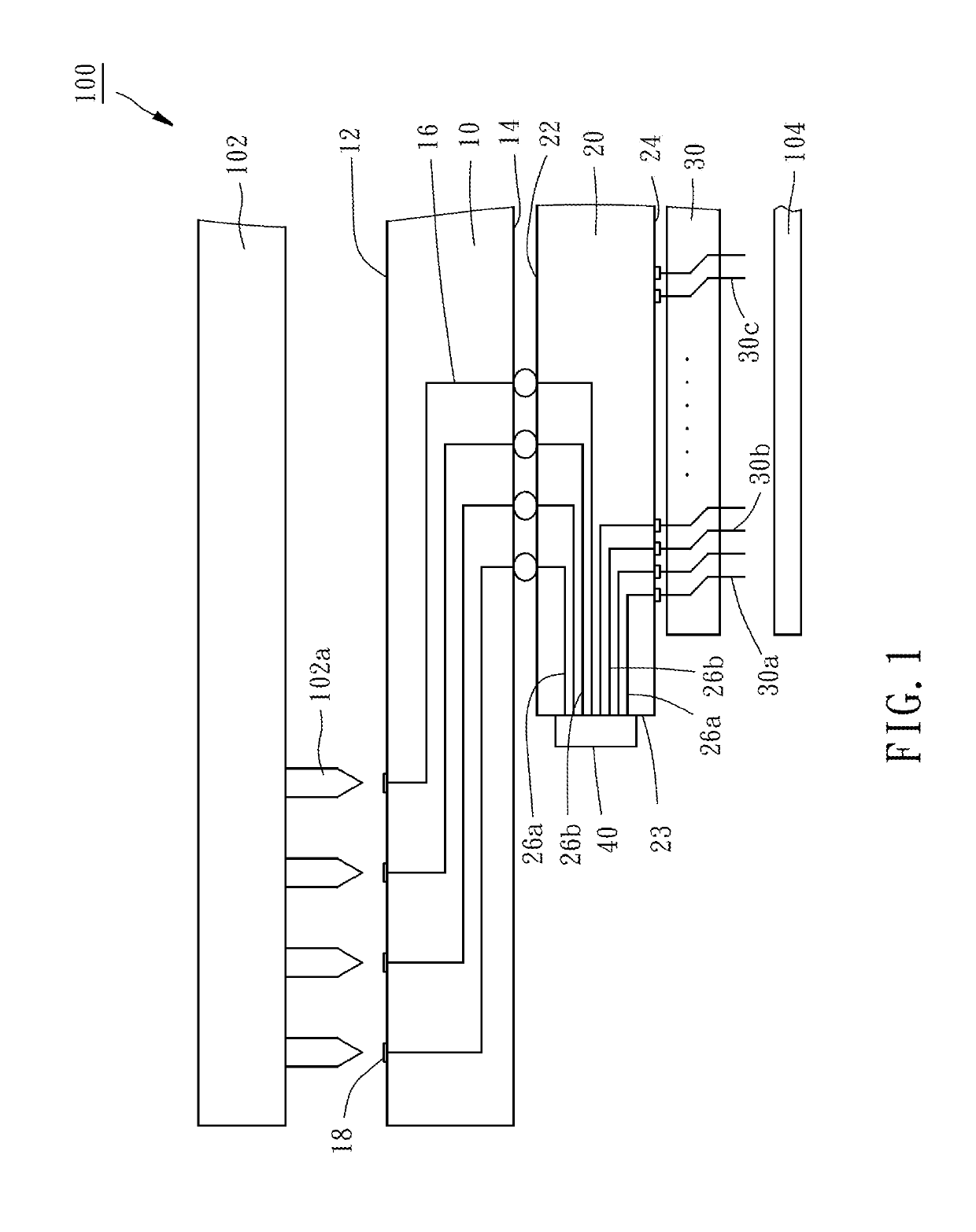
[0027]As shown in FIGS. 1-5, a probe card 100 according to a first embodiment of the present invention primarily includes a printed circuit board 10, a connection substrate 20, a probe head 30, and a signal path switching module 40. The probe card 100 is disposed between a tester 102 and a DUT 104 to serve as a transmission interface for transmitting one or more test signals, such as direct-current or low-frequency signals, from the tester 102 between the tester 102 and the DUT 104 or transmitting one or more loopback test signals, such as high-frequency signals, from the DUT 104 back to the DUT 104.

[0028]The printed circuit board 10 in this embodiment is a general printed circuit board having a top surface 12, a bottom surface 14, a plurality of signal circuit lines 16 located inside the printed circuit board 10, and contact pads formed on the top surface 12 and the bottom surface 14 and electrically connected with the signal circuit lines 16, such as the contact pads 18 that are l...

Example

[0045]Referring to FIGS. 10-11, a probe card 400 according to a fourth embodiment of the present invention as shown in FIG. 10 is provided. The probe card 400 includes a printed circuit board 10, a connection substrate 20, a probe head 30, and a signal channel expanding board 60. The printed circuit board 10, the connection substrate 20 and the probe head 30 used in this embodiment are the same or similar in structural features thereof with that used in the first and second embodiments, so for the detailed structure thereof, the description of the abovementioned embodiments can be referred to.

[0046]Briefly speaking, in this embodiment, the printed circuit board 10 has a top surface 12, a bottom surface 14, and a plurality of signal circuit lines 16 provided between the top and bottom surfaces 12 and 14. The connection substrate 20 has a top surface 22, a bottom surface 24, and a plurality of signal circuit lines provided between the top and bottom surfaces 22 and 24, electrically co...


PUM


Abstract

A probe card includes a printed circuit board (PCB), a connection substrate electrically connected with the PCB, a probe head, and a signal path switching module disposed on a lateral periphery surface or a bottom surface of the connection substrate, electrically connected with probe needles of the probe head and the connection substrate and including first and second circuit lines with first and second inductors respectively, and a capacitor electrically connected between the first and second circuit lines. A test signal from a tester is transmitted between the tester and a device under test (DUT) via the PCB, the connection substrate, the first and second circuit lines and the probe needles. A loopback test signal from the DUT is transmitted back to the DUT via the probe needles, parts of the first and second circuit lines and the capacitor.

Description

BACKGROUND OF THE INVENTION1. Field of the Invention[0001]The present invention relates generally to a probe card and more particularly, to a probe card provided with a signal path switching module, and a signal path switching module assembly used in the probe card.2. Description of the Related Art[0002]A probe card is a transmission interface for transmitting a test signal between a tester and an electronic component under test (hereinafter referred to as “device under test” or “DUT”). It is well known that switching the signal transmission path by relay or circuit composed of capacitors and inductors provided on the probe card enables a same probe needle provided on the probe card to transmit a test signal such as a direct-current or low-frequency signal from the tester or transmit a high-frequency loopback test signal from the DUT. For related prior arts, Taiwan Patent Nos. 1471570, 1474008, 1489113, 1493194 and 1529395 can be referred to.[0003]The electronic components such as t...

Claims


Application Information

Patent Timeline
IPC IPC(8): G01R1/073H05K1/18G01R1/067H05K1/11
CPCG01R1/07385H05K1/181G01R1/07342G01R1/06772G01R1/0675H05K1/111G01R1/07307G01R31/00G01R1/07371G01R31/2889
Inventor WEI, HAOCHOU, CHIA-NANCHEN, CHIEN-CHIAOYU, CHIA-ANCHEN, YU-HAO
Owner MICROELECTRONICS TECH INC
Why Eureka
Try Eureka