Semiconductor device

a technology of semiconductor chip and semiconductor chip, applied in the field of semiconductor chip, can solve the problems of adverse effects adverse influences on the integrated circuit in the semiconductor chip die, etc., and achieve the effect of improving the reliability of an elemen

Active Publication Date: 2019-05-23
SAMSUNG ELECTRONICS CO LTD
View PDF2 Cites 5 Cited by
  • Summary
  • Abstract
  • Description
  • Claims
  • Application Information

AI Technical Summary

Benefits of technology

[0006]An aspect of the present inventive concepts provides a semiconductor device capable of improving re

Problems solved by technology

When dicing of the wafer is performed, chipping, delamination, or micro-cracking may occur, which may cause adverse influences on the integrated circuits in the semiconductor chip

Method used


Image

  • Semiconductor device
  • Semiconductor device
  • Semiconductor device

Examples


Embodiment Construction

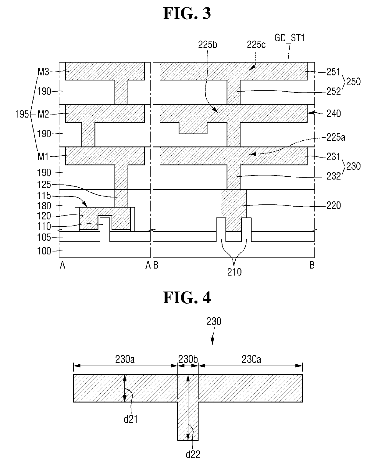
[0034]In the drawings of the semiconductor device according to some example embodiments of the present inventive concepts, a fin type transistor (FinFET) including a channel region of a fin type pattern shape is exemplarily illustrated, but the present inventive concepts are not limited thereto. The semiconductor device according to some example embodiments of the present inventive concepts may include a tunneling FET, a transistor including a nanowire, a transistor including a nanosheet, or a three-dimensional (3D) transistor. The semiconductor device according to some example embodiments of the present inventive concepts may include a planar transistor.

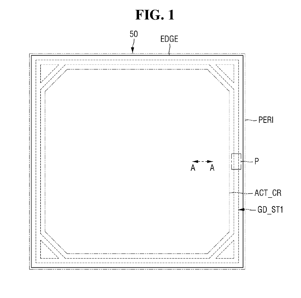
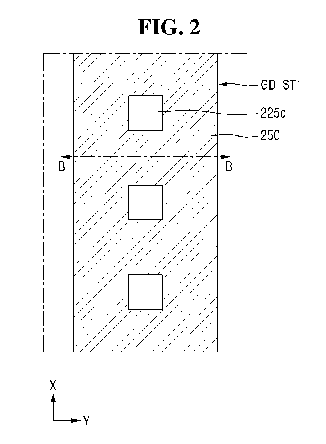
[0035]FIG. 1 is a plan view for explaining the semiconductor device according to some example embodiments of the present inventive concepts. FIG. 2 is an enlarged view of a region P of FIG. 1. FIG. 3 is a cross-sectional view taken along the line A-A of FIG. 1 and the line B-B of FIG. 2. FIG. 4 is a diagram for explaining the first ...


PUM


Abstract

A semiconductor device, comprising: a substrate which includes an active circuit region, and a boundary region surrounding the active circuit region, the boundary region including an edge portion of the substrate; a first lower conductive pattern disposed on the substrate of the boundary region; and a first upper conductive pattern connected to the first lower conductive pattern over the first lower conductive pattern, wherein the first upper conductive pattern includes a first portion having a first thickness, a second portion having a second thickness greater than the first thickness, and a third portion having a third thickness greater than the second thickness, and the third portion of the first upper conductive pattern is connected to the first lower conductive pattern, is provided.

Description

[0001]This application claims priority to Korean Patent Application No. 10-2017-0156422, filed on Nov. 22, 2017, and all the benefits accruing therefrom under 35 U.S.C. § 119, the disclosure of which is incorporated herein by reference in its entirety.BACKGROUND1. Field of the Inventive Concept[0002]The present inventive concepts relate to a semiconductor device, and more specifically, to a semiconductor device including a guide structure which reduces and / or prevents cracks and / or moisture.2. Description of the Related Art[0003]An integrated circuit is a group of electronic circuits on a semiconductor material, which is generally silicon. Semiconductor integrated circuits are manufactured in a front-end process including a photo process, a deposition process and an etching process, which are supplemented by doping and cleaning. Once the front-end process is completed, wafers are prepared for testing and packaging.[0004]Many different packaging techniques have been developed, includ...

Claims


Application Information

Patent Timeline
IPC IPC(8): H01L21/78H01L21/768H01L23/528H01L23/58H01L23/00
CPCH01L21/78H01L21/76816H01L23/5283H01L21/76811H01L23/585H01L23/562H01L23/564H01L2924/3512H01L2924/35121H01L23/5226H01L27/0886H01L23/485H01L24/26H01L29/78H01L29/785
Inventor PARK, JUNG ILAHN, JEONG HOONLEE, JOON-NYUNG
Owner SAMSUNG ELECTRONICS CO LTD
Why Eureka
Try Eureka