
Optical emission spectrometer with cascaded charge storage devices

a charge storage device and optical emission spectrometer technology, applied in the field of optical emission spectrometers, can solve the problems of complicated later modification, limited measurable spectral lines due, and increased production costs with the number of desired spectral lines, and achieves easy comparison, good spectral measurement of the sample, and easy setting up a corresponding dynamic measurement range.

Active Publication Date: 2019-06-06
BRUKER AXS
View PDF0 Cites 0 Cited by
  • Summary
  • Abstract
  • Description
  • Claims
  • Application Information

AI Technical Summary

Benefits of technology

This patent describes a spectrometer that uses cascaded charge storage devices to improve the signal-to-noise ratio when reading the collected charge of a photodiode. By distributing the collected charge over multiple devices with small capacities, the charge component due to one of the devices is enlarged, resulting in better signal-to-noise ratio. This technology also allows for easy setup of a dynamic measurement range, allowing for qualitative good spectral measurement of a sample.

Problems solved by technology

Disadvantages of this construction are the production costs that increase with the number of the desired spectral lines, and the limitation of the measurable spectral lines due to their installation space inside the spectrometer.
In addition, the spectrometer is built for a specific measurement task or application due to the placement of the single channel detectors; later modification is complicated and expensive.
However, a disadvantage is a relatively small dynamic measurement range.
In the case of spectral lines of clearly different intensity, phased exposure times must be used, which requires conversions and results in inaccuracies.
Non-linearities in the dynamic measurement range also falsify the measurement results, which in the case of normalizations results in additional errors, even if a linearization calculation has previously been performed.
In addition, the signal-to-noise ratio is typically relatively poor.
Overall, the determination of intensity ratios and consequently concentration ratios of sample components is difficult.
The prior specification of the amplification for the different pixels is complicated and difficult when the composition of the sample to be examined, and consequently the location and strength of the occurring spectral lines, are not known.

Method used


Image

  • Optical emission spectrometer with cascaded charge storage devices
  • Optical emission spectrometer with cascaded charge storage devices
  • Optical emission spectrometer with cascaded charge storage devices

Examples


Embodiment Construction

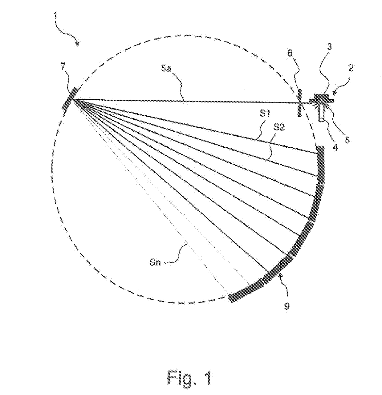
[0046]FIG. 1 shows an embodiment of an optical emission spectrometer 1 according to the invention. The spectrometer 1 comprises an excitation device 2, in the present case what is known as a spark stand, to which a pulsed DC voltage is applied between a sample 3, in the present case a metallic sample which is used as a first electrode, and a mandrel-shaped counter element 4, which is used here as a second electrode. With each DC voltage pulse, a spark discharge occurs between the two electrodes, wherein material is separated from the sample 3 and atoms of the sample material are transformed into a plasma state. Upon re-filling of the electron shells of the atoms, a characteristic emission of light 5 occurs. Typically, between 100 and 2000 spark discharges (also referred to as “sparks”) per second are produced. A typical voltage of the DC voltage is between 3 kV and 10 kV, typically around 5 kV. The individual DC voltage pulse has a length of typically 50 μs to 250 μs, typically arou...


PUM


Abstract

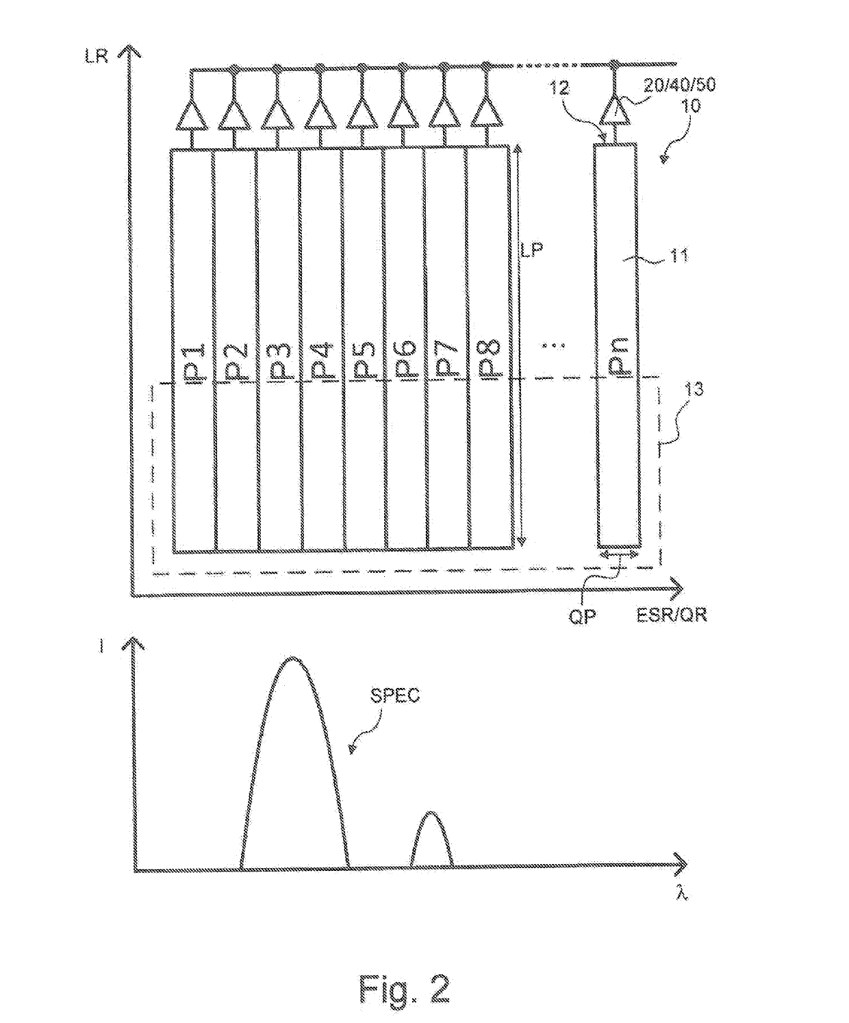
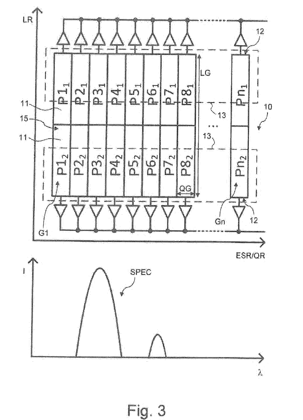
An optical emission spectrometer has an excitation device for a sample to be examined, a dispersive element for spectrally decomposing light emitted by an excited sample, a multiplicity of photodiodes, which are arranged such that different spectral components of the emitted, decomposed light are detectable with different photodiodes, and a multiplicity of electronic readout systems for the photodiodes. A respective electronic readout system has a charge storage assembly comprising a plurality of individual charge storage devices, wherein the charge storage devices are interconnectable in cascading fashion, with the result that charges flowing in from an associated photodiode successively fill the charge storage devices. The respective electronic readout system can be used to read the charges of the individual charge storage devices of the charge storage assembly and / or the charges of subsets of the charge storage devices of the charge storage assembly.

Description

BACKGROUND OF THE INVENTIONField of the Invention[0001]The invention relates to the field of optical emission spectrometers.Description of the Related Art[0002]An optical emission spectrometer of this type is disclosed in U.S. Pat. No. 7,277,170 B2.[0003]Optical emission spectroscopy is a method of instrumental analysis, with which the chemical composition of the sample can be determined qualitatively and quantitatively. With an appropriate excitation, for example spark emission, the atoms present in the sample are excited to emit characteristic electromagnetic radiation (“light”). The emitted light is spectrally decomposed and measured. The chemical composition of the sample can be determined from the position and intensity of the spectral lines.[0004]In a frequently used type of optical emission spectrometer, a plurality of single channel detectors are arranged on a carrier, in accordance with the expected position of spectral lines to be measured, cf. for example DE 20 2014 104 2...

Claims


Application Information

Patent Timeline
Patent Type & Authority Applications(United States)
IPC IPC(8): G01J3/28G01J3/18G01J3/04G01J3/443
CPCG01J3/2803G01J3/18G01J3/04G01J3/443G01J2003/1842G01J3/4406G01J2001/4406G01J2001/446G01J1/46G01J3/20
Inventor WITZIG, ALEXEJVAN STUIJVENBERG, MARTINSIMONS, RAINER
Owner BRUKER AXS
Learn More