Semiconductor device

a technology of semiconductors and devices, applied in the direction of semiconductor devices, basic electric elements, electrical equipment, etc., can solve problems such as deviating formation positions

a technology of semiconductors and devices, applied in the direction of semiconductor devices, basic electric elements, electrical equipment, etc., can solve problems such as deviating formation positions

US20190214457A1Active Publication Date: 2019-07-11FUJI ELECTRIC CO LTD

Image

  • Semiconductor device
  • Semiconductor device
  • Semiconductor device

Examples


embodiment

[0044](Embodiment)

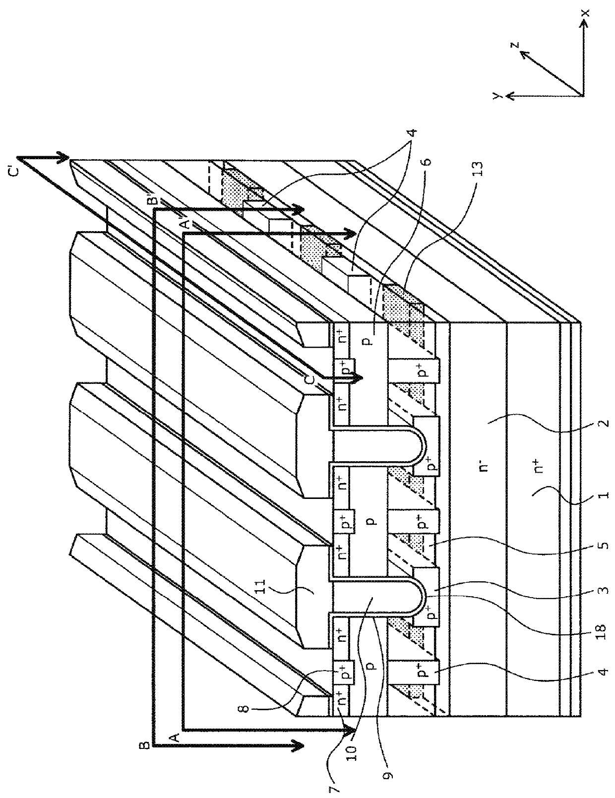
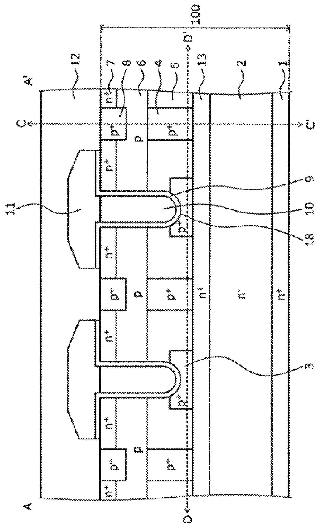
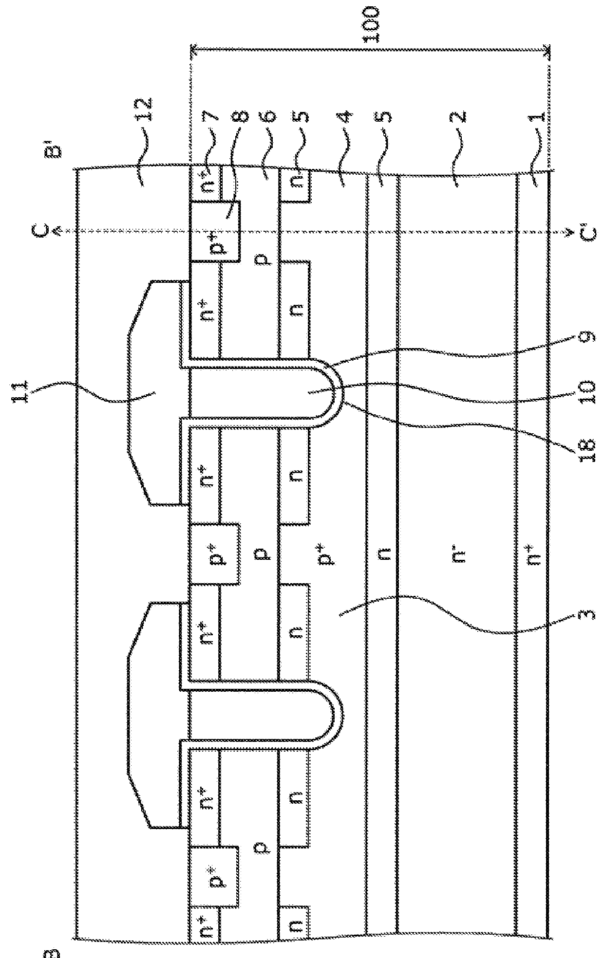
[0045]A semiconductor device according to the present invention is formed using a semiconductor with a wider bandgap than silicon (hereinafter, wide bandgap semiconductor). The description will use a semiconductor device using e.g. silicon carbide (SiC) (silicon carbide semiconductor device) as an example of the wide bandgap semiconductor. FIG. 1 is a perspective view showing a structure of a silicon carbide semiconductor device according to the embodiment of the present invention. FIG. 2 is a cross-sectional view of the A-A′ portion in FIG. 1 that shows the structure of the silicon carbide semiconductor device according to the embodiment. FIG. 3 is a cross-sectional view of the B-B′ portion in FIG. 1 that shows the structure of the silicon carbide semiconductor device according to the embodiment. FIG. 4 is a cross-sectional view of the C-C′ portion in FIG. 1 that shows the structure of the silicon carbide semiconductor device according to the embodiment. FIG. 5 is...


PUM


Abstract

A semiconductor device includes: a semiconductor substrate of a first conductivity type; a first semiconductor layer of the first conductivity type; a second semiconductor layer of a second conductivity type; a first semiconductor region of the first conductivity type; a trench; a second semiconductor region of the second conductivity type; a third semiconductor region of the second conductivity type; and a fourth semiconductor region of the first conductivity type. The second semiconductor region is selectively provided inside the first semiconductor layer, and the third semiconductor region is selectively provided inside the first semiconductor layer and contacts a bottom surface of the trench. The fourth semiconductor region is provided perpendicularly to a lengthwise direction of the trench in a plan view and is located at a depth position that is deeper than the second semiconductor region.

Description

BACKGROUND OF THE INVENTIONTechnical Field[0001]The present invention relates to a semiconductor device.Background Art[0002]Conventionally, in order to reduce the ON resistance of elements in a power semiconductor element, vertical MOSFETs (metal oxide semiconductor field effect transistors) having a trench structure have been fabricated (manufactured). In a vertical MOSFET, the cell density per unit area can be increased more with a trench structure in which the channel is formed perpendicularly to the substrate surface than with a planar structure in which the channel is formed parallel to the substrate surface, which makes it possible to increase current density per unit area and is advantageous from a cost perspective.[0003]However, when the trench structure is formed in a vertical MOSFET, the entire trench inner wall is covered with a gate insulating film in order to form the channel in the vertical direction, and the portion of the gate insulating film on the trench bottom app...

Claims


Application Information

Patent Timeline
11 Jul 2019
Publication
US20190214457A1
IPC
H01L29/06; H01L29/16; H01L29/10; H01L29/78; H01L29/66; H01L21/02; H01L21/04
CPC
H01L29/063; H01L29/1608; H01L29/1095; H01L29/7813; H01L29/66068; H01L21/02529; H01L21/046; H01L21/049
Inventors
KINOSHITA, AKIMASA; OKUMURA, KEIJI