Vertical probe card

a probe card and vertical probe technology, applied in the direction of printed circuit parts, printed circuit non-printed electric components association, instruments, etc., can solve the problems of limited test time and affect the accuracy of test, and achieve the effect of shortening the signal transmission distance and reducing the loss of signal during transmission

Active Publication Date: 2019-08-15
SUZHOU TAOSHENG ELECTRONICS TECH CO LTD
View PDF0 Cites 1 Cited by
  • Summary
  • Abstract
  • Description
  • Claims
  • Application Information

AI Technical Summary

Benefits of technology

[0025]A signal can be transmitted by the vertical probe card provided by the embodiment of the present disclosure without having to pass through the entire probe, shortening the signal transmission distance and thereby reducing signal loss during transmission through the probe. This vertical probe card is particularly suitable for high frequency signal transmission.

Problems solved by technology

The signal is transmitted through the test probe, but a signal loss caused by the resistance or inductance of the test probe itself affects the accuracy of the test, especially in a high frequency test (for example, a signal frequency used in the test is 10-40 GHz) where a larger signal attenuation is caused and the test is limited.

Method used


Image

  • Vertical probe card
  • Vertical probe card
  • Vertical probe card

Examples


Embodiment Construction

[0034]The disclosure is further described in conjunction with the following embodiments and accompanying drawings.

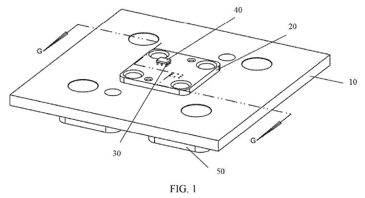
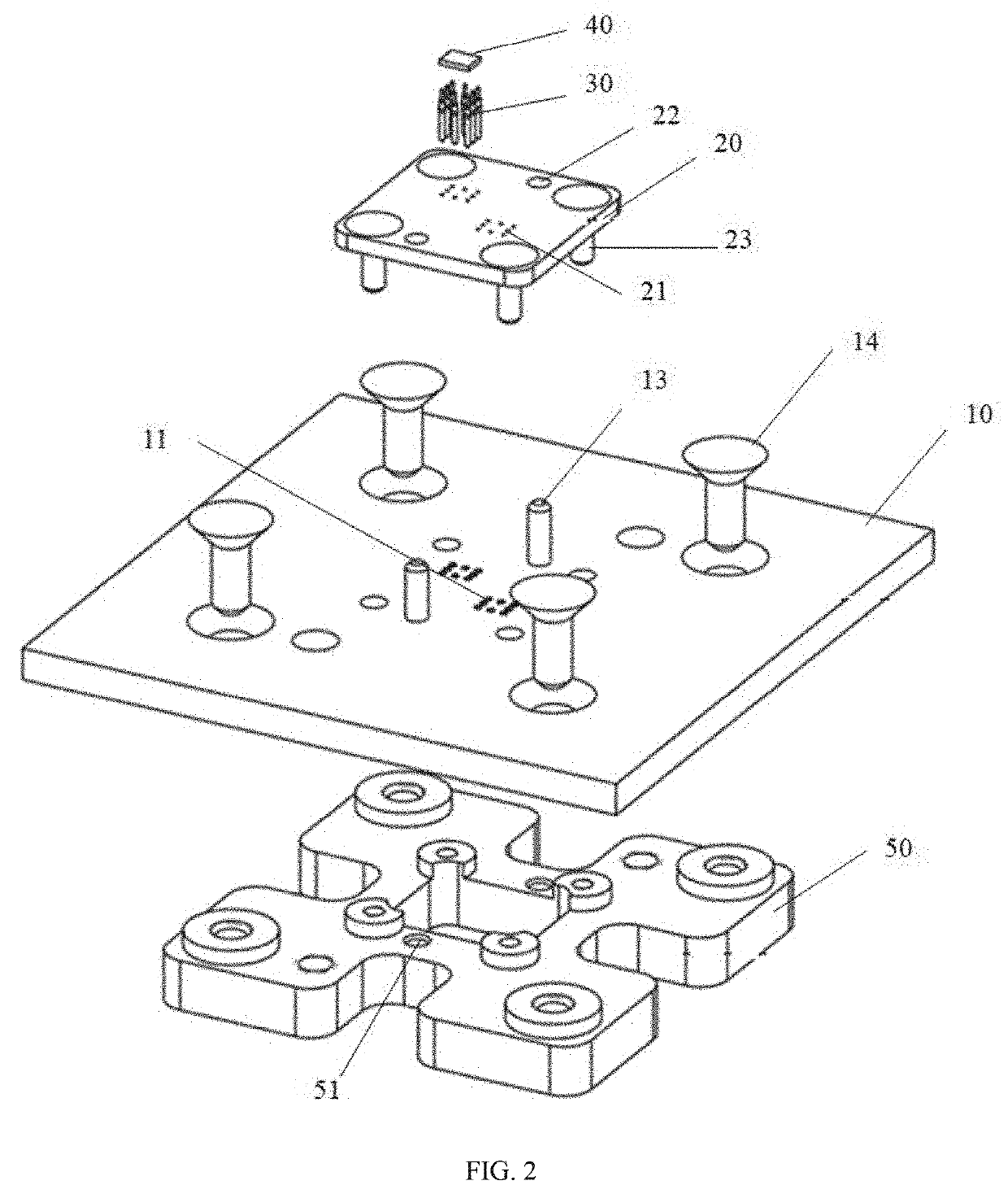
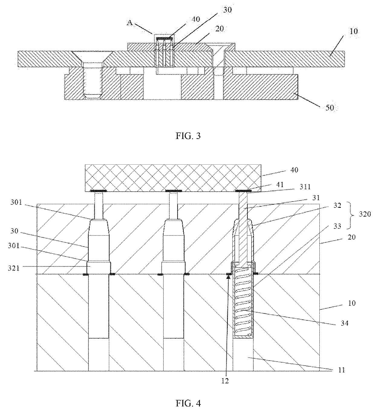
[0035]Referring to FIGS. 1-5, an embodiment provides a vertical probe card for performing EDS on a chip to determine whether the chip is qualified before the chip is packaged. The vertical probe card includes a PCB 10, a cover plate 20 and a probe 30.

[0036]Referring to FIGS. 2 and 4, the PCB 10 includes a substrate, and the substrate is provided with a bottom hole 11 and a PCB pad 12 surrounding the bottom hole 11. It can be understood that the substrate may be one of various PCB substrates in the existing art, and usually these substrates are made of insulating materials. Optionally, the substrate is one of a bakelite plate, a glass fiberboard, and various plastic sheets. In some other embodiments, the substrate may also be a composite sheet of multi-layer materials, such as a sheet-like material in which glass fibers, non-woven materials and resin are laminated.

[0037]T...


PUM


Abstract

Provided is a vertical probe card, the vertical probe card includes: a printed circuit board (PCB) including a bottom hole and a PCB pad surrounding the bottom hole; a cover plate disposed on the PCB and including a cover hole, where the cover hole and the bottom hole are disposed coaxial with each other and form a receiving space; and a probe received in the receiving space. The probe includes a probe head passing through the cover hole to extend out of the cover plate and to contact with a chip, where an end, which is provided with the probe head, of the probe is a first end; and a protruding portion disposed in the mid-portion of the probe and in contact with the PCB pad, where a part between the probe head and the protruding portion of the probe and the protruding portion are conductors.

Description

CROSS-REFERENCES TO RELATED APPLICATIONS[0001]This application claims priority to PCT Application No. PCT / CN2017 / 109587, filed on Nov. 6, 2017, which is based upon and claims priority to Chinese Patent Application No. 201710352127.3, filed on May 18, 2017, the entire contents both of which are incorporated herein by reference.FIELD OF TECHNOLOGY[0002]The following relates to a probe card technology field, for example, to a vertical probe card.BACKGROUND[0003]Before a chip is packaged, an electrical die sorting (EDS) is usually performed. According to an EDS test result, a qualified chip can be packaged. The EDS is implemented by a tester equipped with various measurement software and test instruments and a prober station loaded with probe cards. During the test, each probe of a probe card is in direct contact with a die pad of a wafer to achieve electrical connection between the die pad of the wafer and the tester, thereby achieving a purpose of testing electrical characteristics of...

Claims


Application Information

Patent Timeline
Patent Type & Authority Applications(United States)
IPC IPC(8): G01R1/073H05K1/11H05K1/18G01R1/067
CPCG01R1/07314H05K1/111H05K1/182G01R1/06733G01R1/06716H05K2201/10151G01R1/06755G01R1/06772G01R1/0408G01R1/07307G01R1/07342G01R1/07378G01R3/00G01R31/2601G01R31/2889
Inventor SHI, YUANJUNLIU, KAI
Owner SUZHOU TAOSHENG ELECTRONICS TECH CO LTD
Why Eureka
Try Eureka