Methods and systems for optical functionalisation of a sample made of semiconductor material

Active Publication Date: 2019-08-29
UNIV DE PROVENCE D AIX MARSEILLE I +1
View PDF0 Cites 0 Cited by
  • Summary
  • Abstract
  • Description
  • Claims
  • Application Information

AI Technical Summary

Benefits of technology

The patent describes a process that allows for the control of the refractive index of a material, which can prevent damage and enable the inscription of optical functions. By controlling the variation of the real part of the refractive index, the process limits the relative variation of the refractive index to a value less than 0.1 in absolute value. Additionally, the process measures the imaginary part of the refractive index to ensure that it remains below 10−3 in absolute value.

Problems solved by technology

However, to date, no optical functionalization technology similar to those known for dielectric materials has been demonstrated in the volume of monolithic semiconductor materials, particularly in silicon.
This is also due to the importance of non-linear effects during the propagation and absorption of light in semiconductor materials, which intrinsically limit femtosecond laser energy deposition to a level insufficient for material modification (see for example A. Mouskeftaras et al.
Although SOI technology provides excellent optical performance, it nevertheless has major disadvantages, specific to lithography.
A first disadvantage is that the manufactured waveguides are contained in a plane (i.e., 2D), which prevents the design of three-dimensional architectures for the optical functionalization of the material.
A second disadvantage is that this technique requires several steps in a clean and controlled environment in order to avoid problems related to unwanted external pollution.
However, no technique seems to have demonstrated tangible results allowing direct inscription of optical waveguides deep in a semiconductor material, which would open the door to optical functionalization by direct 3D laser writing in semiconductor materials, and in particular in silicon.

Method used


Image

  • Methods and systems for optical functionalisation of a sample made of semiconductor material
  • Methods and systems for optical functionalisation of a sample made of semiconductor material
  • Methods and systems for optical functionalisation of a sample made of semiconductor material

Examples


Embodiment Construction

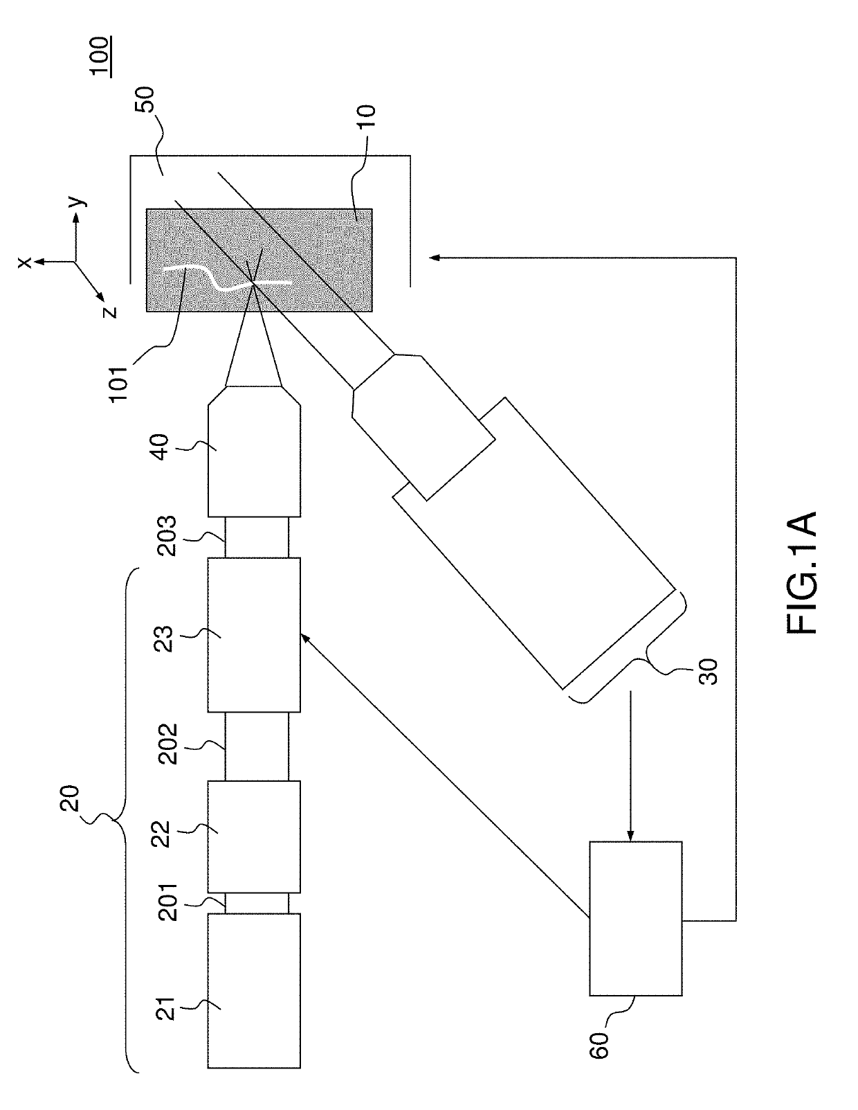
[0074]FIG. 1 illustrates a first example of a laser marking system 100 for deep optical functionalization in a sample 10 of semiconductor material, as described here.

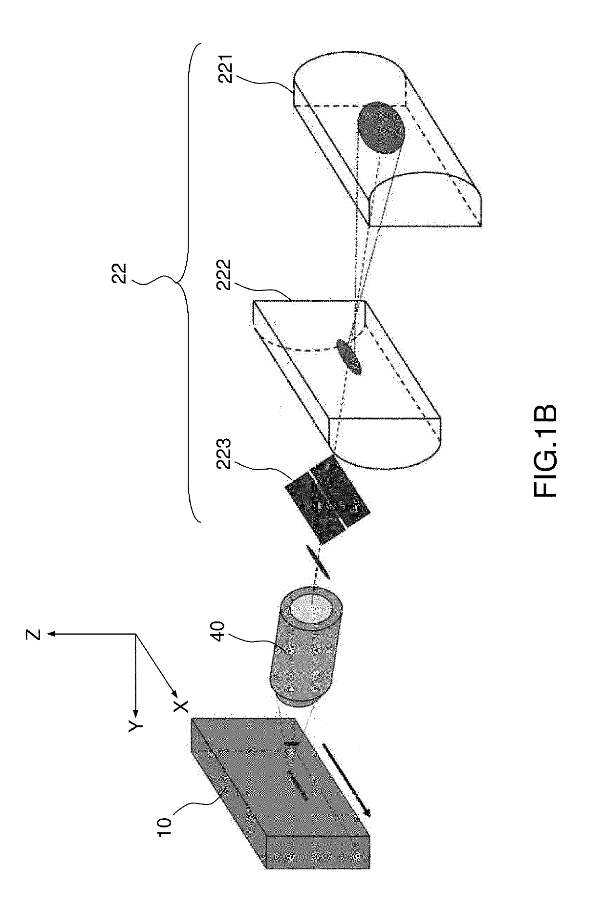
[0075]The laser marking system 100 includes, in particular, an emission source 20 of a laser beam 203 formed of pulses and a focusing system 40 for focusing of the laser beam in the sample (e. g. a microscope objective, a converging lens, a parabolic mirror, etc.). The resulting focal volume can be moved deep into the sample in a pattern 101 by means of relative means of movement 50 of the laser beam and the sample. In the example of FIG. 1A, the relative means of displacement 50 include a plate for moving the sample along the 3 axes X, Y, Z. However, each of the translations can be replaced by an optical device adapted to the movement of the beam, for example a lens called a “f-theta lens”. System 100 also includes a device 30 for measuring the real part of the refractive index in the sample and a control unit 60 of th...


PUM


Abstract

According to one aspect, the invention concerns a system (100) for the in-depth optical functionalization of a sample (10) made of semiconductor material, comprising:a source (20) for emitting a laser beam formed by pulses of effective duration between 1 ps and 100 ns, having a wavelength in the spectral transparency band of the material;a microscope objective (40) for deep focusing in the sample of the laser beam in a predetermined pattern, the light intensity per pulse in a focal volume of the laser beam being adapted for multiphoton absorption in the semiconductor material;a device (30) for measuring the real part of the refractive index of the sample at each point of the pattern;a control unit (60) for controlling the number of pulses received per pattern point as a function of said measurement of the real part of the refractive index so as to obtain, at each pattern point, a progressive modification of the real part of the refractive index of the material until a relative variation of the real part of the refractive index greater than 10−3 in absolute value is obtained.

Description

STATE OF THE ARTTechnical Field of the Invention[0001]This invention concerns processes and systems for deep optical functionalization of a sample of semiconductor material, including the three-dimensional inscription of optical waveguides deeply in the sample.State of the Art[0002]The emergence of femtosecond laser sources has made it possible to develop well-controlled direct 3D laser writing technologies in transparent dielectric materials such as glass, particularly for applications involving the “optical functionalization” of the material, particularly by writing optical waveguides. Optical functionalization is achieved by controlled variation of the real part of the refractive index in dielectric materials (see for example K. M. Davis et al. “Writing waveguides in glass with a femtosecond laser”, Opt. Letters, Vol. 21, Nr 21 (1996)).[0003]However, to date, no optical functionalization technology similar to those known for dielectric materials has been demonstrated in the volum...

Claims


Application Information

Patent Timeline
IPC IPC(8): G02B6/13G02B6/122B23K26/53
CPCG02B6/13G02B6/122G02B21/02G02B2006/12107B23K26/53G02B2006/12102
Inventor GROJO, DAVIDCHAMBONNEAU, MAXIME
Owner UNIV DE PROVENCE D AIX MARSEILLE I
Why Eureka
Try Eureka