System on chip (SOC) builder

a technology of system on chip and builder, which is applied in the direction of cad circuit design, instrumentation, and semiconductor/solid-state device details. it can solve the problems of complex routing form, inability to analyze and implement, and the number of components on the chip is rapidly growing. it facilitates the incorporation of building block circuits, reduces the amount of data, and improves system efficiency.

Active Publication Date: 2019-08-29
INTEL CORP
View PDF0 Cites 9 Cited by
  • Summary
  • Abstract
  • Description
  • Claims
  • Application Information

AI Technical Summary

Benefits of technology

[0028]Aspects of the present disclosure relate to methods, systems, and computer readable mediums for overcoming the above-mentioned issues with existing implementations of generating topology for a given SoC by significantly improving system efficiency by facilitating efficient creation of SoC designs utilizing existing or new circuit block information. The system and method assist a designer to design SoC in a convenient manner and facilitate incorporation of building block circuits previously tested in silicon. The system and method reduces the amount of data a user has to enter manually to adequately describe features of the circuit being designed or analyzed
[0029]Further, methods, systems, and computer readable mediums are provided that facilitates efficient and effe...

Problems solved by technology

The number of components on a chip is rapidly growing due to increasing levels of integration, system complexity and shrinking transistor geometry.
In heterogeneous mesh topology in which one or more routers or one or more links are absent, dimension order routing may not be feasible between certain source and destination nodes, and alternative paths may have to be taken.
This form of routing may be complex to analyze and implement.
Based upon the traffic between various end points, and the routes and physical networks that are used for various messages, different physical channels of the NoC interconnect may experience different levels of load and congestion.
Unfortunately, channel widths cannot be arbitrarily large due to physical hardware design restrictions, such as timing or wiring congestion.
There may be a limit on the maximum channel width, thereby putting a limit on the maximum bandwidth of any single NoC channel.
Additionally, wider physical channels may not help in achieving higher bandwidth if messages are short.
Due to these limitations on the maximum NoC channel width, a channel ...

Method used


Image

  • System on chip (SOC) builder
  • System on chip (SOC) builder
  • System on chip (SOC) builder

Examples


Embodiment Construction

[0073]The following detailed description provides further details of the figures and example implementations of the present application. Reference numerals and descriptions of redundant elements between figures are omitted for clarity. Terms used throughout the description are provided as examples and are not intended to be limiting. For example, the use of the term “automatic” may involve fully automatic or semi-automatic implementations involving user or administrator control over certain aspects of the implementation, depending on the desired implementation of one of ordinary skill in the art practicing implementations of the present application.

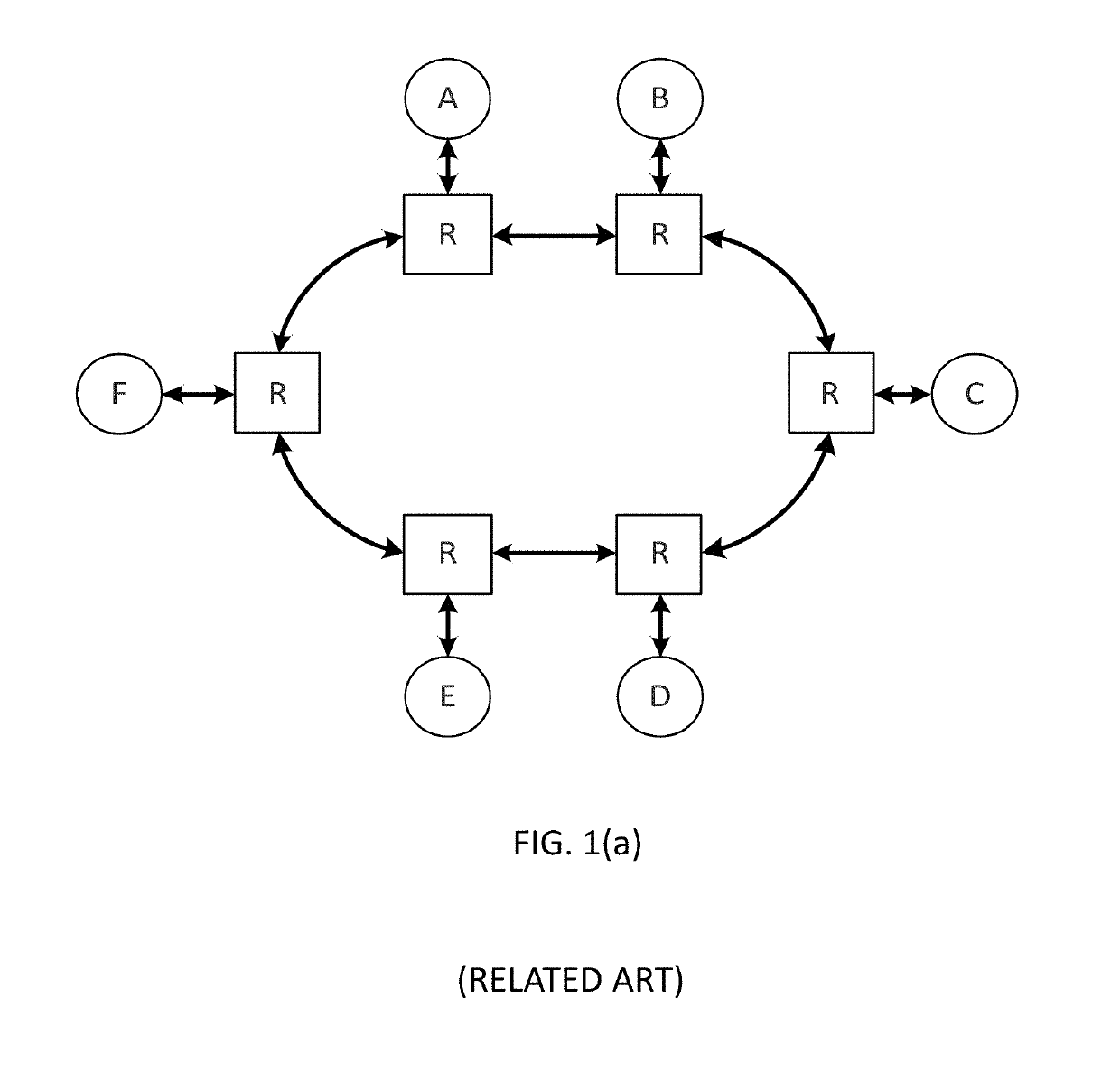
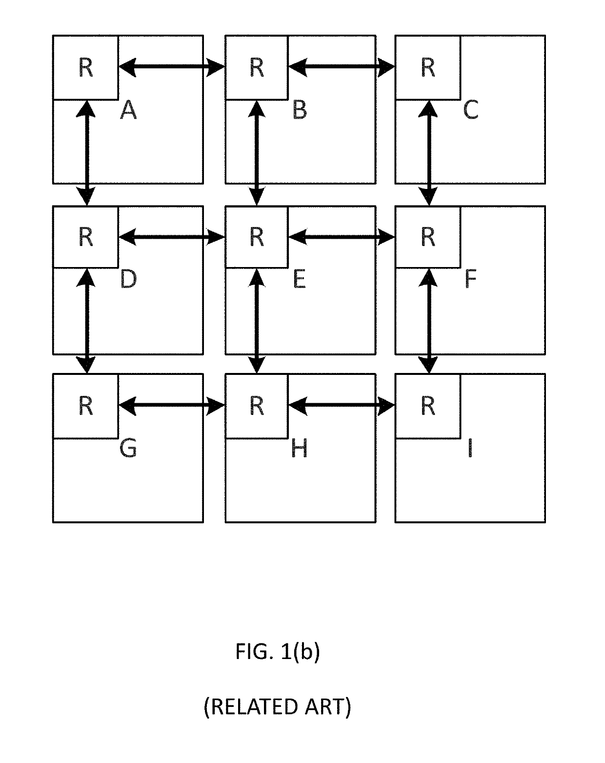
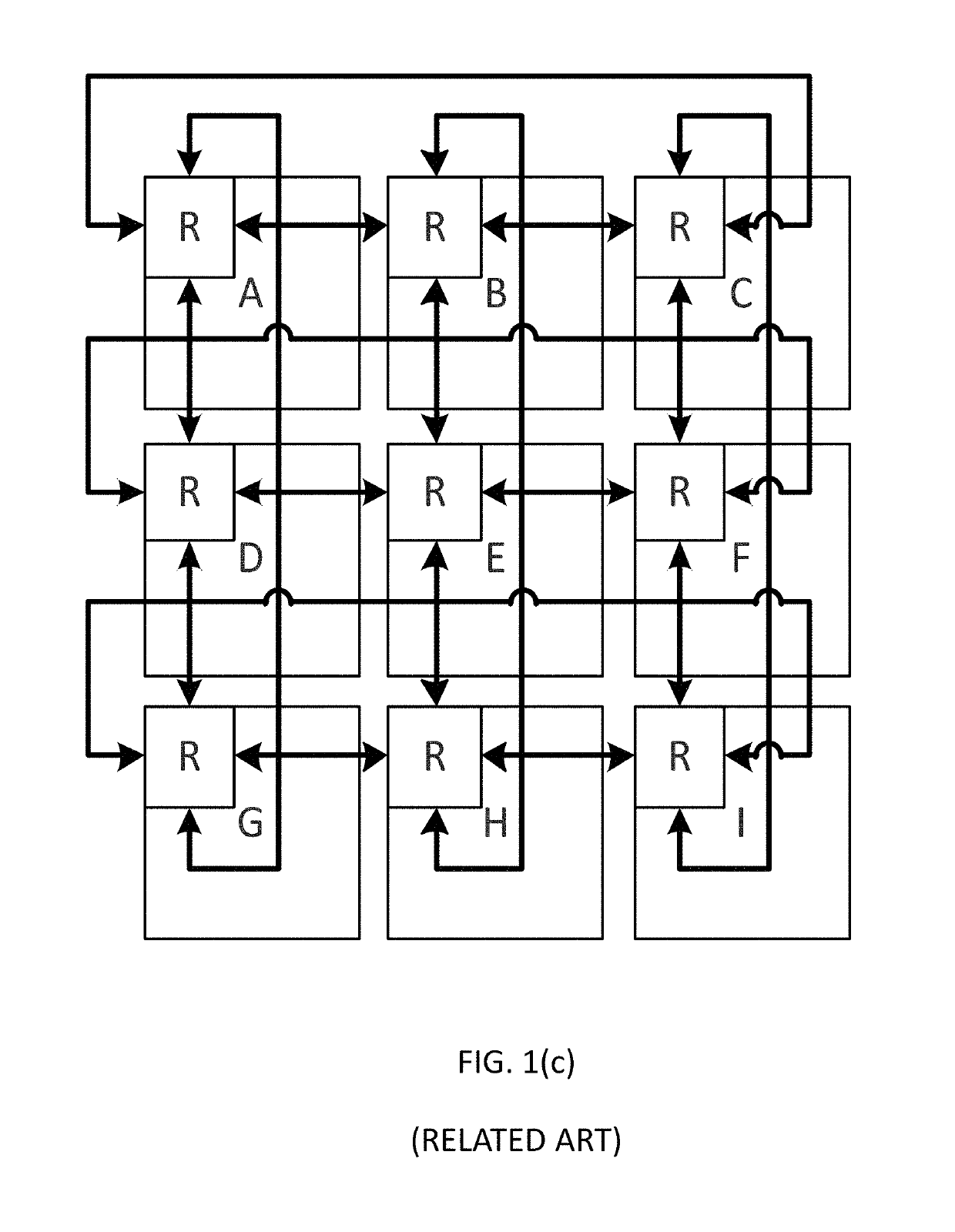
[0074]Network-on-Chip (NoC) has emerged as a paradigm to interconnect a large number of components on the chip. NoC is a global shared communication infrastructure made up of several routing nodes interconnected with each other using point-to-point physical links. In example implementations, a NoC interconnect is generated from a specific...


PUM


Abstract

Methods and example implementations described herein are generally directed to a System on Chip (SoC) design and verification system and method that constructs SoC from functional building blocks circuits while concurrently taking into account numerous chip level design aspects along with the generation of a simulation environment for design verification. An aspect of the present disclosure relates to a method for generating a System on Chip (SoC) from a floor plan having one or more integration descriptions. The method includes the steps of generating one or more connections between the integration descriptions of the floor plan based at least on a traffic specification, and conducting a design check process on the floor plan. If the design check process on the floor plan is indicative of passing the design check process, then the method generates the SoC according to the one or more connections generated between the integration descriptions.

Description

CROSS REFERENCE TO RELATED APPLICATION[0001]This U.S. patent application is based on and claims the benefit of domestic priority under 35 U.S.C. 119(e) from provisional U.S. patent application No. 62 / 634,653, filed on Feb. 23, 2018, the disclosures of which is hereby incorporated by reference herein in its entirety.BACKGROUNDField[0002]Methods and example implementations described herein are generally directed to an interconnect architecture, and more specifically, to System on Chip (SoC) design and verification system and method that constructs SoC from functional building blocks circuits while concurrently taking into account numerous chip level design aspects along with the generation of a simulation environment for design verification.Related Art[0003]The number of components on a chip is rapidly growing due to increasing levels of integration, system complexity and shrinking transistor geometry. Complex System-on-Chips (SoCs) may involve a variety of components e.g., processor ...

Claims


Application Information

Patent Timeline
IPC IPC(8): G06F17/50H01L23/31
CPCG06F17/5072G06F17/5045G06F17/5022H01L23/3114G06F30/30G06F30/33G06F30/392
Inventor RAO, NISHANTKUMAR, SAILESHRAPONI, PIER GIORGIO
Owner INTEL CORP
Why Eureka
Try Eureka