

Method for manufacturing element chip
a manufacturing method and element chip technology, applied in the direction of semiconductor/solid-state device testing/measurement, electric discharge tubes, semiconductor devices, etc., can solve the problems of defective product as an element chip, difficult to stick the mask completely along the uneven portions, and debris from the gap may enter the mask and stick to the front surface of the substrate, etc., to achieve the effect of easy removal
- Summary
- Abstract
- Description
- Claims
- Application Information
AI Technical Summary
Benefits of technology
Problems solved by technology
Method used
Image

Examples
first embodiment
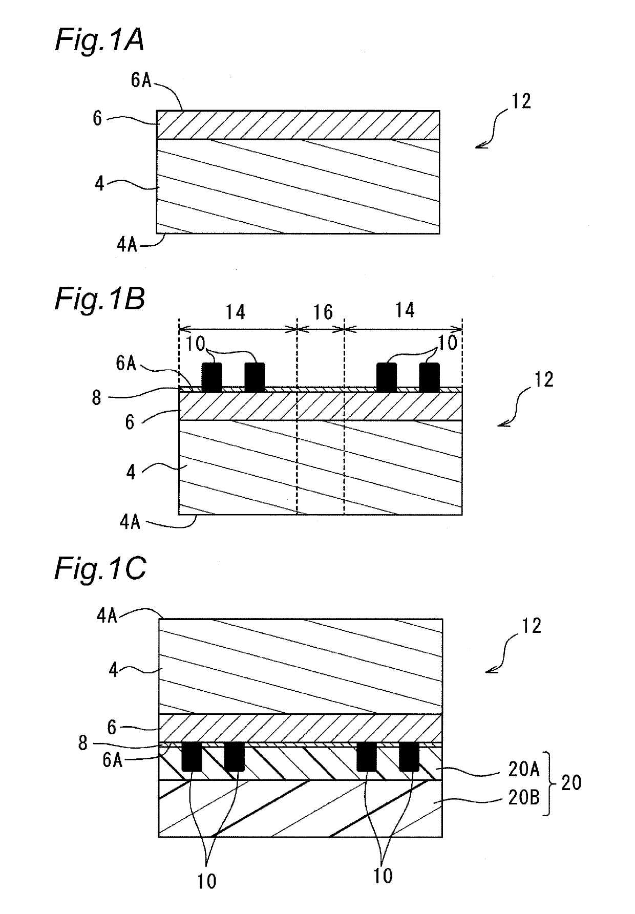
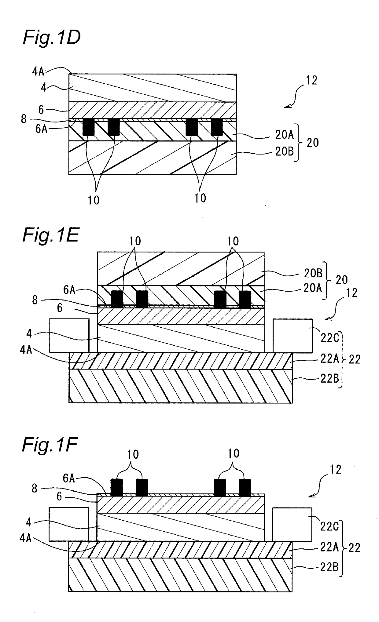
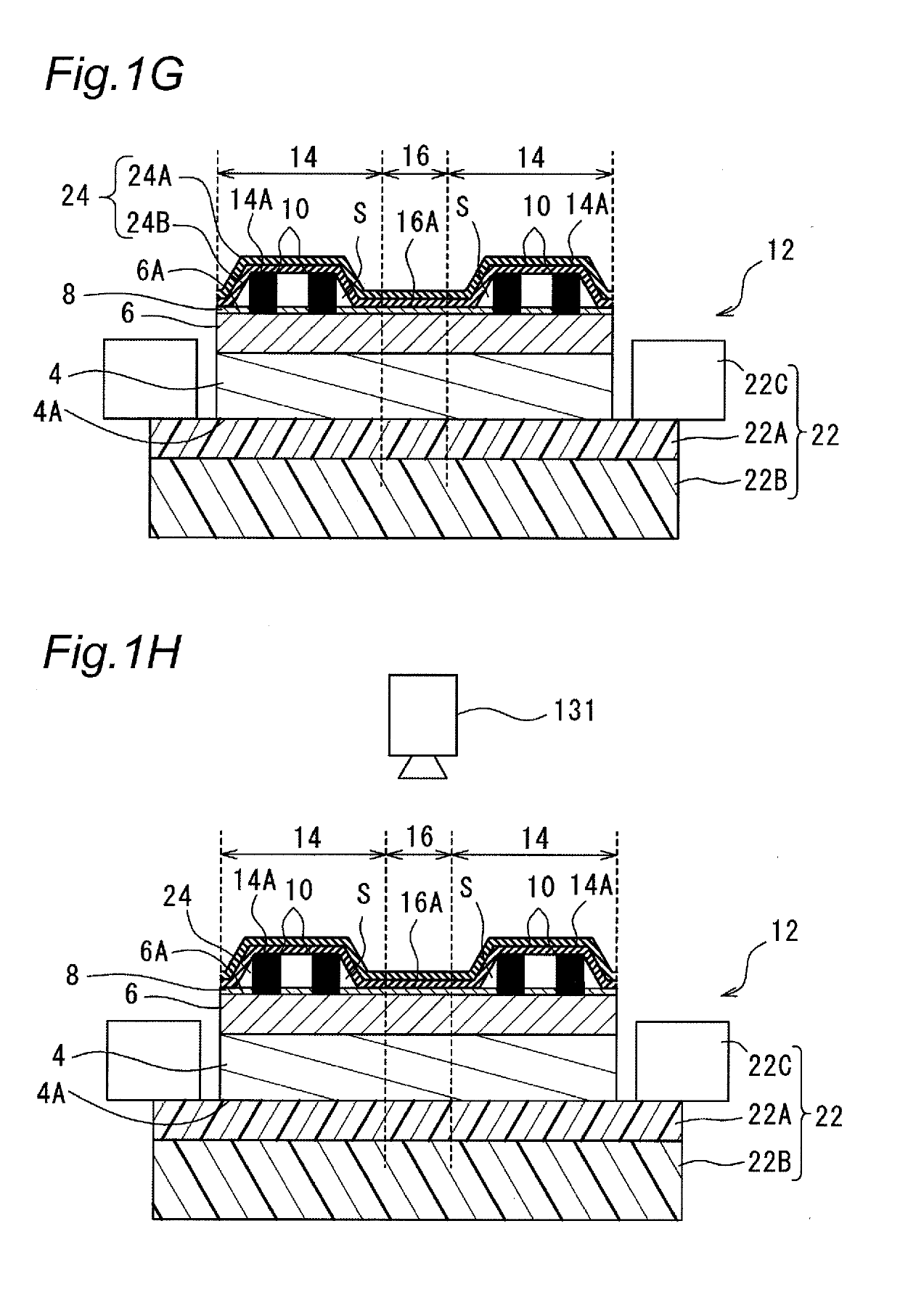
[0053]FIGS. 1A to 1K show manufacturing steps of a semiconductor chip (element chip) 2 according to the first embodiment of the present invention. Referring to FIG. 1K being a completed drawing, the manufactured semiconductor chip 2 includes a semiconductor layer 4, a wiring layer 6 formed on the semiconductor layer 4, a protective film 8 formed on the wiring layer 6, and bumps 10 as electrodes. The semiconductor layer 4 is made of, for example, Si or a Si-based material, and the wiring layer 6 is made of, for example, an insulating film such as SiO2 and metal such as Cu. The material of the insulating film of the wiring layer 6 may be SiN, SiOC, Low-k material, or the like. In addition, the material of the metal of the wiring layer 6 may be Al, Al alloy, W, or the like. In addition, TEG is also included in the wiring layer 6. In addition, the metal contained in the bump 10 may be copper; an alloy of copper, tin, and silver; an alloy of silver and tin; an alloy of lead and tin; gold...
second embodiment
[0084]FIGS. 6A to 6F show respective manufacturing steps in a method for manufacturing a semiconductor chip (element chip) 2 according to the second embodiment. FIGS. 6A to 6F respectively show a first mask forming step, a second mask forming step, a measuring step, a laser scribing step, a dicing step, and a mask removing step. It should be noted that the first preparation step, the second preparation step, the protection step, the thinning step, the first holding step, and the second holding step in the first embodiment are also executed in the present embodiment as in the first embodiment, but since the contents are the same, the description thereof will be omitted. In addition, also in the first mask forming step, the second mask forming step, the measuring step, the laser scribing step, the dicing step, and the mask removing step, descriptions of the same contents as those in the first embodiment may be omitted.
[0085]In the first mask forming step shown in FIG. 6A, an adhesive ...
third embodiment
[0090]A method for manufacturing a semiconductor chip 2 of the present embodiment is substantially the same as that of the first embodiment except the mask forming step. Therefore, description of parts similar to those of the first embodiment will be omitted. First, as in the first embodiment, the first preparation step (FIG. 1A), the second preparation step (FIG. 1B), the protection step (FIG. 1C), the thinning step (FIG. 1D), the first holding step (FIG. 1E), and the second holding step (FIG. 1F) are sequentially performed.
[0091]In the first mask forming step shown in FIG. 7A, a water-soluble resin 23 is applied onto the front surface of a semiconductor wafer 12. The resin 23 is applied to reduce the level difference on the front surface of the semiconductor wafer 12. Spray coating or spin coating can be adopted as the application method of the resin 23. In the present embodiment, since bumps 10 are formed in an element region 14, the height of the element region 14 is higher than...
PUM
 Abstract
Description
Claims
Application Information