Electroconductive film, touch panel, and image display device

a touch panel and electroconductive film technology, applied in the direction of solid-state devices, conductive layers on insulating supports, synthetic resin layered products, etc., can solve the problems of low surface resistance low haze value of electroconductive film, and inability to achieve the effect of preventing the reduction of electrical conductivity, low haze value, and low surface resistance valu

Active Publication Date: 2019-10-03
DAI NIPPON PRINTING CO LTD
View PDF0 Cites 2 Cited by
  • Summary
  • Abstract
  • Description
  • Claims
  • Application Information

AI Technical Summary

Benefits of technology

[0030]According to the first aspect of the present invention, an electroconductive film can achieve a low haze value and a low surface resistance value and prevent reduction in electrical conductivity due to the reaction of the electroconductive fibers with substances in the atmosphere, since the electroconductive part comprises a light-transmitting resin and plural electroconductive fibers incorporated in the light-transmitting resin; the electroconductive part can conduct electricity from the surface of the electroconductive part; the electroconductive fibers as a whole are unevenly distributed on the light-transmitting base material side than the position located at half the film thickness of the electroconductive part in the electroconductive part; the electroconductive part has a surface resistance value of 200Ω / □ or less; and the electroconductive film has a haze value of 5% or less. According to the second aspect of the present invention, an electroconductive film that can achieve a low haze value and low surface resistance value and has reduced the difference in electrical resistance depending on the in-plain direction of the electroconductive part can be provided, since the ratio of the electrical resistance in a first direction to that in a second direction is 1 or more and less than 2 when the electrical resistance values on the surface of the electroconductive part are measured in a predetermined size in six different directions including an arbitrary direction for each an angle of 30 degrees to the arbitrary direction in the surface of the electroconductive part, wherein a direction in which the electroconductive part shows the lowest electrical resistance value is designated as the first direction, and a direction which is perpendicular to the first direction is designated as the second direction; the electroconductive part has a surface resistance value of 200Ω / □ or less; and the electroconductive film has a haze value of 5% or less. According to the third aspect of the present invention, an electroconductive film that can achieve a low haze value and a low surface resistance value and has flexibility can be provided, since an electroconductive part is provided directly on at least one surface of a light-transmitting resin base material; the electroconductive part has a surface resistance value of 200Ω / □ or less; and the electroconductive film has a haze value of 5% or less. According to the fourth aspect of the present invention, an electroconductive film that can achieve a low haze value and a low surface resistance value and has flexibility and can increase choices of electroconductive pastes can be provided, since underlayer is provided directly on at least one surface of a light-transmitting resin base material; an electroconductive part is provided directly on the underlayer; the electroconductive part has a surface resistance value of 200Ω / □ or less; and the electroconductive film has a haze value of 5% or less. Additionally, according to a touch panel and an image display device of other aspects of the present invention, a touch panel and an image display device comprising such the electroconductive film can be provided.

Problems solved by technology

Because of this problem, an electroconductive film having a low haze value and a low surface resistance value has not yet been obtained.
However, when an electroconductive film is formed by using metallic nanowires, a difference in electrical resistance depending on the in-plain direction or area of an electroconductive part occurs.
If the electrical resistance is different depending on the in-plain direction or area of the electroconductive part and the electroconductive film is used as an electrode for a touch panel sensor, the patterning of the electrode and / or the resulting IC chips may be limited, as well as the electroconductive film is limited in imposition and is thus prone to be wasted.

Method used


Image

  • Electroconductive film, touch panel, and image display device
  • Electroconductive film, touch panel, and image display device
  • Electroconductive film, touch panel, and image display device

Examples


first embodiment

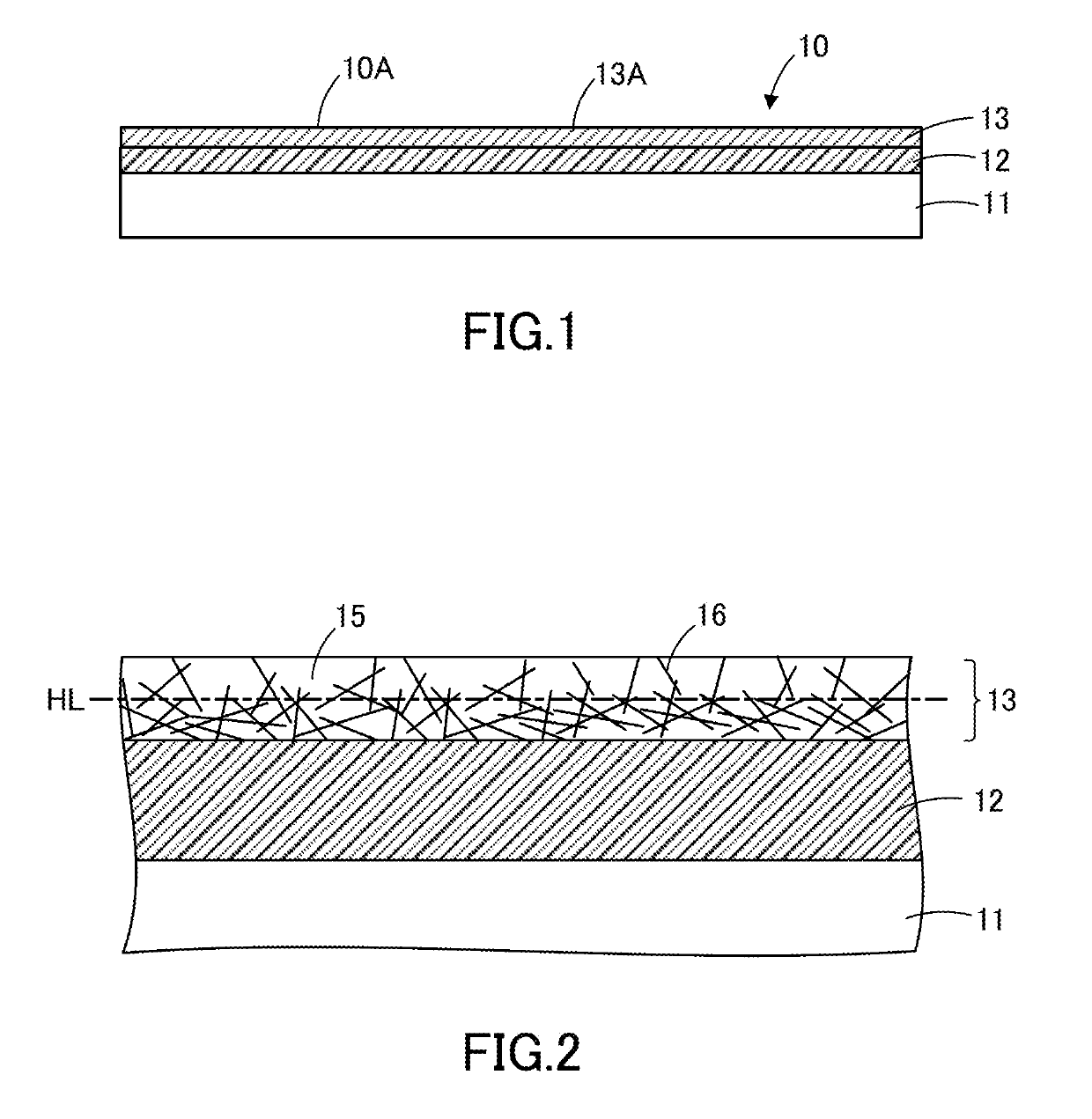
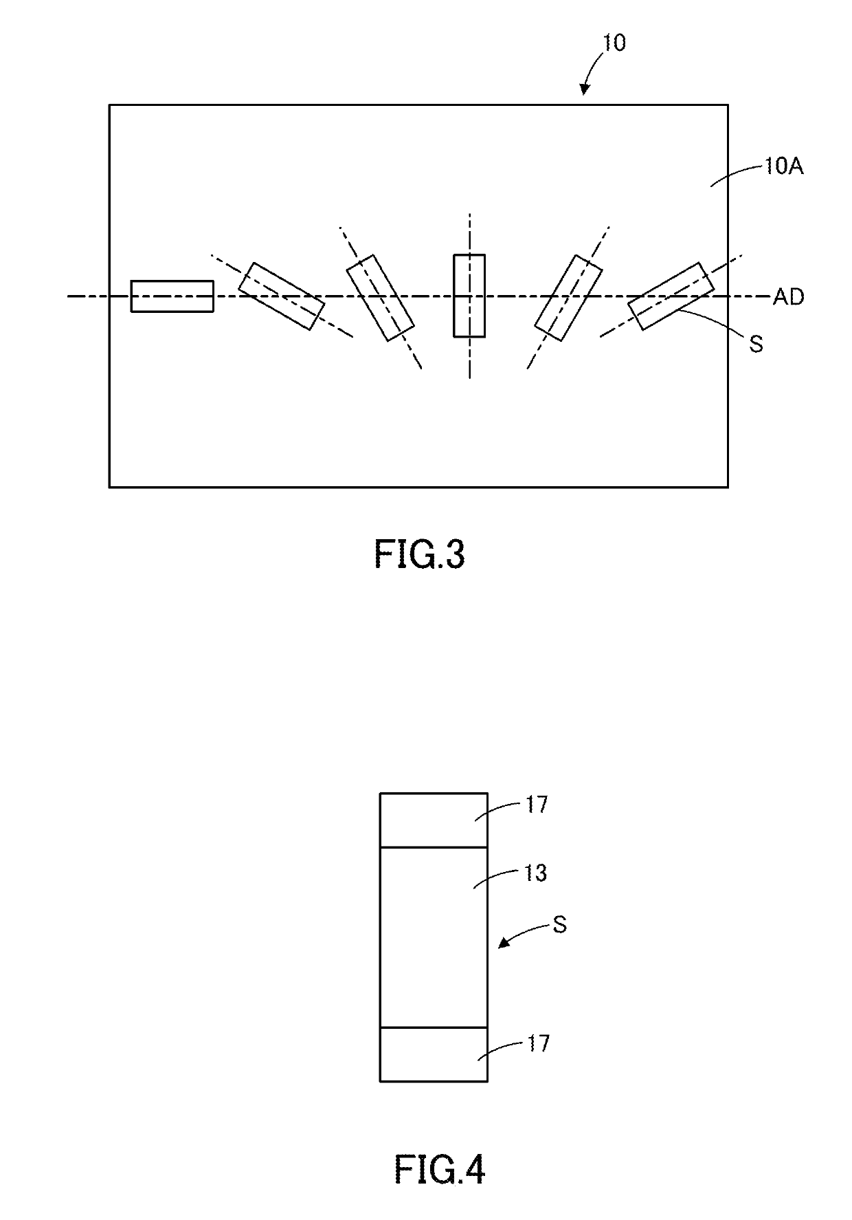
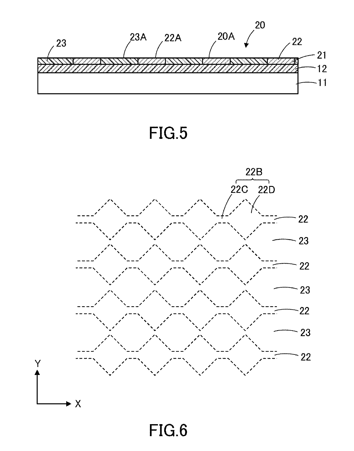
[0066]Now, the electroconductive film, touch panel, and image display device according to the first embodiment of the present invention will be described below with reference to the drawings. The term “light-transmitting” as used herein refers to a property of transmitting light. Additionally, the term “light-transmitting” does not necessarily refer to transparency and may refer to translucency. FIG. 1 depicts a schematic diagram of an electroconductive film according to the present embodiment, while FIG. 2 depicts an enlarged view of a part of the electroconductive film shown in FIG. 1. FIG. 3 depicts a layout drawing of samples excised from the electroconductive film according to the present embodiment, while FIG. 4 depicts a plain view of a sample measured for electrical resistance. FIGS. 5 and 8 depict schematic diagrams of other electroconductive films according to the present embodiment; FIG. 6 depicts a schematic plain view of the electroconductive film shown in FIG. 5; FIG. ...

second embodiment

[0240]Now, the electroconductive film, touch panel, and image display device according to the second embodiment of the present invention will be described below with reference to the drawings. FIG. 16 depicts a schematic diagram of an electroconductive film according to the present embodiment; FIG. 17 depicts an enlarged view of a part of the electroconductive film shown in FIG. 16; FIG. 18 depicts a schematic diagram of another electroconductive film according to the present embodiment; and FIG. 19 depicts an enlarged view of a part of the electroconductive film shown in FIG. 18.

>>

[0241]The electroconductive film 100 shown in FIG. 16 is light transmissive and comprises a light-transmitting base material 101, a light-transmitting functional layer 102 provided on one surface of the light-transmitting base material 101, and an electroconductive part 103 provided on a surface of the light-transmitting functional layer 102 opposite to the light-transmitting base material 101 side surfac...

third embodiment

[0290]Now, the electroconductive film, touch panel, and image display device according to the third embodiment of the present invention will be described below with reference to the drawings. FIG. 21 depicts a schematic diagram of an electroconductive film according to the present embodiment; FIG. 22 depicts an enlarged view of a part of the electroconductive film shown in FIG. 21; and FIG. 23 schematically illustrates each step of the foldability test. FIG. 24 depicts a schematic diagram of another electroconductive films according to the present embodiment, while FIG. 25 depicts an enlarged view of a part of the electroconductive film shown in FIG. 24. FIGS. 26 and 27 schematically illustrate the process for producing the electroconductive film according to the present embodiment.

>>

[0291]The electroconductive film 150 shown in FIG. 21 is light transmissive and comprises a light-transmitting base material 151, and an electroconductive part 152 provided directly on one surface of th...


PUM

PropertyMeasurementUnit
hazeaaaaaaaaaa
light transmittanceaaaaaaaaaa
lengthaaaaaaaaaa

Abstract

One aspect of the present invention provides a light-transmitting electroconductive film 10 comprising a light-transmitting base material 11 and an electroconductive part 13 provided on one surface of the light-transmitting base material 11, wherein the electroconductive part 13 includes a light-transmitting resin 15 and plural electroconductive fibers 16 incorporated in the light-transmitting resin 15, and the electroconductive part 13 can conduct electricity from the surface 13A of the electroconductive part 13, and the electroconductive fibers 16 as a whole are unevenly distributed on the light-transmitting base material side than the position HL, which is located at half the film thickness of the electroconductive part 13 in the electroconductive part 13, and the electroconductive part 13 has a surface resistance value of 200 Ω / □ or less, and the electroconductive film 10 has a haze value of 5% or less.

Description

CROSS-REFERENCE TO RELATED APPLICATION[0001]The present application enjoys the benefit of priority to the prior Japanese Patent Application Nos. 2016-195230 (filed on Sep. 30, 2016), 2016-195231 (filed on Sep. 30, 2016), 2016-195233 (filed on Sep. 30, 2016), 2016-195234 (filed on Sep. 30, 2016), and 2017-74413 (filed on Apr. 4, 2017), the entire disclosures of which are incorporated herein by reference.TECHNICAL FIELD[0002]The present invention relates to an electroconductive film, a touch panel, and an image display device.BACKGROUND ART[0003]Recent image display devices such as smartphone and tablet terminal may comprise a touch panel system that enables direct input of information by touching an image display screen with a finger or the like.[0004]A touch panel typically comprises an electroconductive film that comprises an electroconductive part provided on a light-transmitting base material and indium tin oxide (ITO) is mainly used as an electroconductive material for such elec...

Claims


Application Information

Patent Timeline
Patent Type & Authority Applications(United States)
IPC IPC(8): G06F3/044G06F3/041H01L51/44H01L27/32
CPCG06F2203/04111G06F2203/04112H01L27/323G06F3/0412H01L51/442G06F3/044B32B27/18B32B27/08B32B23/08B32B2307/546B32B27/40B32B2255/10B32B23/00B32B2255/26B32B2260/021B32B27/281B32B27/30B32B27/34B32B27/32B32B27/38B32B2307/40B32B27/36B32B25/14B32B2264/102B32B25/08B32B7/12B32B2264/105B32B2262/02B32B2307/202B32B2262/106B32B27/308B32B2262/103B32B2260/046B32B2457/208B32B27/304B32B27/302B32B2307/20G06F3/0446H10K59/40H10K71/621B32B7/025B32B27/20H01B5/14B32B7/02H10K30/82
Inventor OGUMI, SHOICHIROOGAWA, YOSHIMASAOOISHI, EIJIIWATA, YUKIMITSUSHIMIZU, YUJIKITAYAMA, RYOTAMUTOU, HIROAKI
Owner DAI NIPPON PRINTING CO LTD
Why Eureka
Try Eureka