Method for forming transparent conductive pattern

A technology of transparent conductivity and transparent conductivity, which is applied in the direction of conductive pattern formation, conductive materials, conductive materials, etc., can solve problems affecting conductive performance, metal nanowires and/or metal nanotube damage, and achieve the effect of reducing damage

Active Publication Date: 2018-12-21
RESONAC CORP
View PDF9 Cites 0 Cited by
  • Summary
  • Abstract
  • Description
  • Claims
  • Application Information

AI Technical Summary

Problems solved by technology

[0009] In this method, depending on the conditions of screen printing, metal nanowires and / or metal nanotubes will be damaged during repeated printing, and this damage will affect the electrical conductivity.

Method used


Image

  • Method for forming transparent conductive pattern
  • Method for forming transparent conductive pattern
  • Method for forming transparent conductive pattern

Examples


Embodiment 1

[0088]

[0089] Polyvinylpyrrolidone K-90 (manufactured by Nippon Catalyst Co., Ltd.) (0.49 g), AgNO 3 (0.52g) and FeCl 3 (0.4 mg) was dissolved in ethylene glycol (125 ml), and a heating reaction was carried out at 150° C. for 1 hour. The obtained precipitate was separated by centrifugation, and the precipitate was dried to obtain the target silver nanowire (average diameter 36 nm, average length 20 μm). The above ethylene glycol, AgNO 3 and FeCl 3 It is manufactured by Wako Pure Chemical Industry Co., Ltd.

[0090]

[0091] After adding 6 times the volume of dibutyl ether to the reaction solution of the silver nanowires obtained by performing a heating reaction at 150° C. for 1 hour and stirring, the nanowires were allowed to stand still to precipitate. After the nanowires were precipitated, the supernatant was separated by decantation, thereby performing solvent replacement to obtain a suspension of silver nanowires dispersed in dibutyl ether (viscosity adjusting so...

Embodiment 2

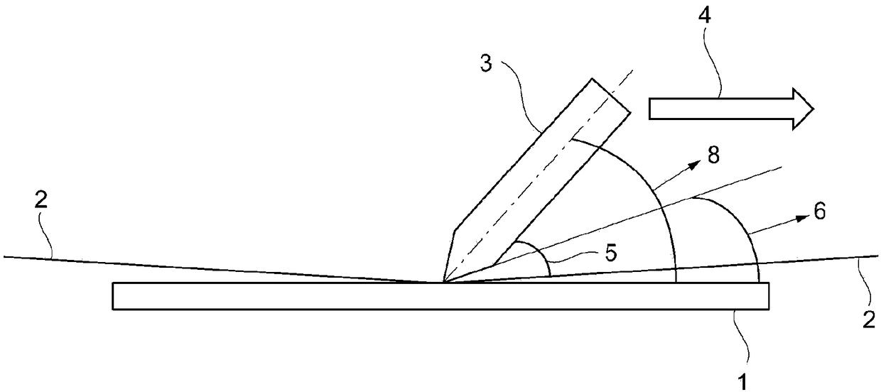
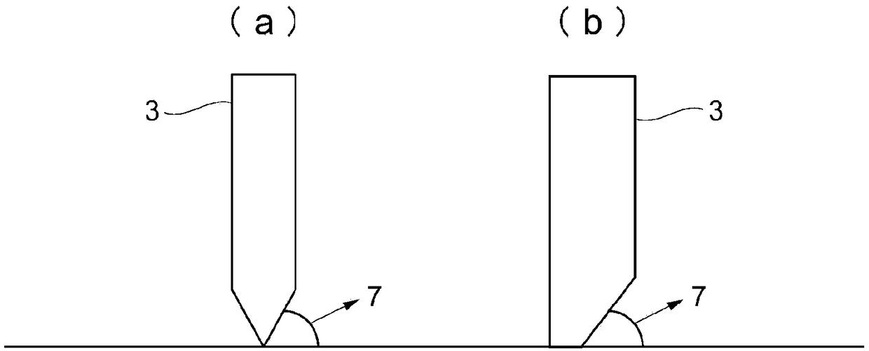
[0100] Instead of attaching the squeegee at an attachment angle of 60°, the squeegee was attached at an attachment angle of 65°, and printed in the same manner as in Example 1. In this embodiment, by installing the scraper at an installation angle of 65°, the angle of attack at the top end of the scraper becomes 30°.


PUM

PropertyMeasurementUnit
viscosityaaaaaaaaaa
thicknessaaaaaaaaaa
wavelengthaaaaaaaaaa

Abstract

The subject of the invention provides a method for forming a transparent conductive pattern that reduces damage to metal nanowires and / or metal nanotubes during screen printing using a transparent conductive ink containing metal nanowires and / or metal nanotubes as a conductive component and thereby makes it possible to form a transparent conductive pattern via a simple production process while minimizing production costs and environmental impact. The attack angle of a squeegee tip section that is brought into contact with a screen mask (2) is set in the range of 1-30 degrees when screen printing with a transparent conductive ink (5) containing a dispersion medium and at least one of metal nanowires and metal nanotubes.

Description

technical field [0001] The invention relates to a method for forming a transparent conductive pattern. Background technique [0002] Transparent conductive film is used in liquid crystal display (LCD), plasma display panel (PDP), organic electroluminescent device (OLED), solar cell (PV) and transparent electrode of touch screen (TP), antistatic (ESD) film and electromagnetic wave shielding ( (1) low surface resistance, (2) high light transmittance, and (3) high reliability are required for use in various fields such as EMI) film. [0003] For example, for a transparent electrode of an LCD, it is suitable that the surface resistance is in the range of 10-300Ω / □, and the light transmittance is more than 85% in the visible light range. A more preferable range is that the surface resistance is 20 to 100Ω / □, and the light transmittance is 90% or more. For the transparent electrode of the OLED, it is suitable that the surface resistance is in the range of 10-100Ω / □, and the ligh...

Claims


Application Information

Patent Timeline
Patent Type & Authority Applications(China)
IPC IPC(8): H01B13/00B41M1/12C09D11/037C09D11/52H01B1/00H01B1/22H05K3/12
CPCB41M1/12C09D11/037C09D11/52H01B1/00H01B1/22H01B13/00H05K3/12H05K3/1216
Inventor 若林正一郎山木繁
Owner RESONAC CORP
Why Eureka
Try Eureka