Three-dimensional vertical NOR Flash Thin-Film Transistor Strings

a transistor string and three-dimensional vertical technology, applied in semiconductor devices, semiconductor/solid-state device details, instruments, etc., can solve the problems of limiting affecting the performance of the transistor, and reducing the number of transistors that can be programmed in parallel, so as to reduce the sensitivities to read disturbance, reduce the cost per bit, and reduce read-latency

Active Publication Date: 2019-10-17
SUNRISE MEMORY CORP
View PDF0 Cites 50 Cited by
  • Summary
  • Abstract
  • Description
  • Claims
  • Application Information

AI Technical Summary

Benefits of technology

[0026]Organizing the TFTs as vertical NOR strings—rather than the prior art vertical NAND strings—results in (i) a reduced read-latency that can approach that of a dynamic random access memory (DRAM) array, (ii) reduced sensitivities to read-disturb and program-disturb conditions that are associated with long NAND Flash strings, and (iii) reduced cost per bit, as compared to a NAND Flash string.
[0027]According to an alternative embodiment of the present invention, each active column in the memory structure includes one or more vertical NOR strings, with each NOR string having thin-film storage transistors sharing a local source line and a local bit line, the local bit line is connected by one segment of a segmented global bit line to a sense amplifier provided in the semiconductor substrate. To significantly reduce the read sense latency, rather than a global bit line that spans a substantial distance (e.g., between a half to the complete length of the chip), multiple, shorter global bit line segments are provided. Each such global segment connects one or more neighboring local bit lines through a segment connector to a segment sense amplifier provided in the semiconductor substrate. In embodiments in which the local source lines are pre-charged to a virtual ground voltage (e.g., Vss), the parasitic capacitance of the virtual ground is increased substantially by providing a short global source line segment connector which connects a group of neighboring local source lines into one local source line segment. The number of local source lines included in the segment determines the combined parasitic capacitance (C).

Problems solved by technology

Thin film NAND transistors have lower conductivity than NAND transistors formed in single crystal silicon, therefore the low read current that is required to be conducted through a long string of NAND TFTs results in a relatively slow read access (i.e. long latency).
Channel hot-electron injection programming requires a relatively large electron current to flow through the channel region, therefore limiting the number of transistors that can be programmed in parallel.
Fowler-Nordheim tunneling and direct tunneling are orders of magnitude more efficient than channel hot-electron injection, allowing massively parallel programming; however, such tunneling is more susceptible to program-disturb conditions.
Furthermore, the polysilicon thin films upon which a vertical NAND string is formed have much lower channel mobility—and therefore higher resistivity—than conventional NAND strings formed in a single-crystal silicon substrate, thereby resulting in a low read current relative to the read current of a conventional NAND string.

Method used


Image

  • Three-dimensional vertical NOR Flash Thin-Film Transistor Strings
  • Three-dimensional vertical NOR Flash Thin-Film Transistor Strings
  • Three-dimensional vertical NOR Flash Thin-Film Transistor Strings

Examples


Embodiment Construction

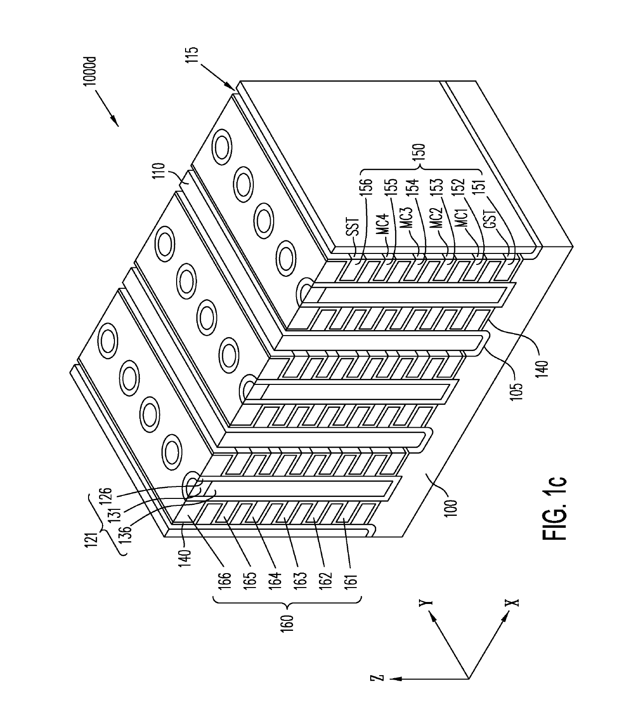
[0059]FIG. 2 shows conceptualized memory structure 100, which illustrates a 3-dimensional organization of memory cells (or storage elements) provided in vertical NOR strings. In conceptualized memory structure 100, each vertical NOR string includes memory cells that are each controlled by a corresponding horizontal word line, according to one embodiment of the present invention. In conceptualized memory structure 100, each memory cell is formed in deposited thin films provided “vertically”, i.e., along a direction perpendicular to the surface of substrate layer 101. Substrate layer 101 may be, for example, a conventional silicon wafer used for fabricating integrated circuits, familiar to those of ordinary skill in the art. In this detailed description, a Cartesian coordinate system (such as indicated in FIG. 2) is adopted solely for the purpose of facilitating discussion. Under this coordinate system, the surface of substrate layer 101 is considered a plane which is parallel to the ...


PUM


Abstract

A memory structure, includes active columns of polysilicon formed above a semiconductor substrate, each active column includes one or more vertical NOR strings, with each NOR string having thin-film storage transistors sharing a local source line and a local bit line, the local bit line is connected by one segment of a segmented global bit line to a sense amplifier provided in the semiconductor substrate.

Description

CROSS REFERENCE TO RELATED APPLICATIONS[0001]The present application is a continuation of U.S. patent Application, Ser. No. 16 / 252,304, entitled “Three-dimensional vertical NOR Flash Thin-Film Transistor Strings,” filed Jan. 18, 2019, which is a continuation-in-part application of co-pending U.S. patent application (“Non-Provisional Application I”), Ser. No. 16 / 107,732, entitled “Three-dimensional vertical NOR Flash Thin-Film Transistor Strings,” filed on Aug. 21, 2018, which is a continuation application of U.S. patent application Ser. No. 15 / 837,734 entitled “Three-dimensional vertical NOR Flash Thin-Film Transistor Strings,” filed on Dec. 11, 2017, now U.S. Pat. No. 10,096,364, which is a divisional application of U.S. patent application Ser. No. 15 / 343,332, entitled “Three-dimensional vertical NOR Flash Thin-Film Transistor Strings,” filed on Nov. 4, 2016, now U.S. Pat. No. 9,842,651, which claims priority of (i) U.S. provisional patent application (“Provisional Application I”),...

Claims


Application Information

Patent Timeline
Patent Type & Authority Applications(United States)
IPC IPC(8): H01L27/11582H01L29/10G11C16/04H01L27/11565H01L23/532H01L23/522G11C16/26G11C16/14G11C16/30H01L27/1157H01L27/11573H01L29/786H01L23/528H01L29/06
CPCH01L27/11582H01L27/11573H01L29/78642H01L23/528G11C16/14G11C16/26H01L29/1037G11C16/0483H01L27/1157H01L23/53257H01L23/5329H01L23/5226G11C16/30H01L29/0649H01L27/11565G11C16/0466G11C16/32G11C16/08H01L29/78696H01L29/40117H10B43/10H10B43/20H10B43/27H10B43/35H10B43/40
Inventor HARARI, ELI
Owner SUNRISE MEMORY CORP
Why Eureka
Try Eureka