Stacked device, stacked structure, and method of manufacturing stacked device

a technology of stacked devices and stacked structures, applied in semiconductor devices, semiconductor/solid-state device details, electrical devices, etc., can solve problems such as the failure of another semiconductor element, and achieve excellent heat dissipation and bonding strength

Active Publication Date: 2019-11-28
FUJIFILM CORP
View PDF0 Cites 7 Cited by
  • Summary
  • Abstract
  • Description
  • Claims
  • Application Information

AI Technical Summary

Benefits of technology

[0024]According to the present invention, a bonding s

Problems solved by technology

In a case where semiconductor elements or the like are stacked as described above, heat ge

Method used


Image

  • Stacked device, stacked structure, and method of manufacturing stacked device
  • Stacked device, stacked structure, and method of manufacturing stacked device
  • Stacked device, stacked structure, and method of manufacturing stacked device

Examples


example 1

[0555]In a test substrate 90 illustrated in FIG. 78, a silicon oxide insulating layer was formed on a surface of a silicon substrate, and terminals 92 were formed on the silicon oxide insulating layer as illustrated in FIG. 78 such that an area ratio of the terminals 92 on a surface 91 including the terminals 92 in a plan view was 45%. The terminals 92 were formed of copper.

[0556]The test substrate 90 was prepared through the following processes (i) to (vi).

[0557](i) Using a photolithography method, a resist pattern of the terminals 92 was formed on the surface of the silicon substrate as illustrated in FIG. 78 such that the area ratio of the terminals 92 on the surface 91 including the terminals 92 in a plan view was 45%.

[0558](ii) A sheet layer as a starting point of plating was provided in the resist opening (recess portion) of the resist pattern.

[0559](iii) The resist opening was plated with metal.

[0560](iv) The resist was stripped, and the terminals were arranged on the silicon...

example 2

[0566]Example 2 was the same as Example 1, except that the bonding configuration was surface activated bond (SAB).

example 3

[0567]Example 3 was the same as Example 1, except that the recess amount was 80 nm, the bonding configuration was SAB, a sealing resin was used during the bonding of the test substrates 90. As described above, by changing the treatment time of dry etching, the recess amount was controlled. The sealing resin will be described below in detail.


PUM


Abstract

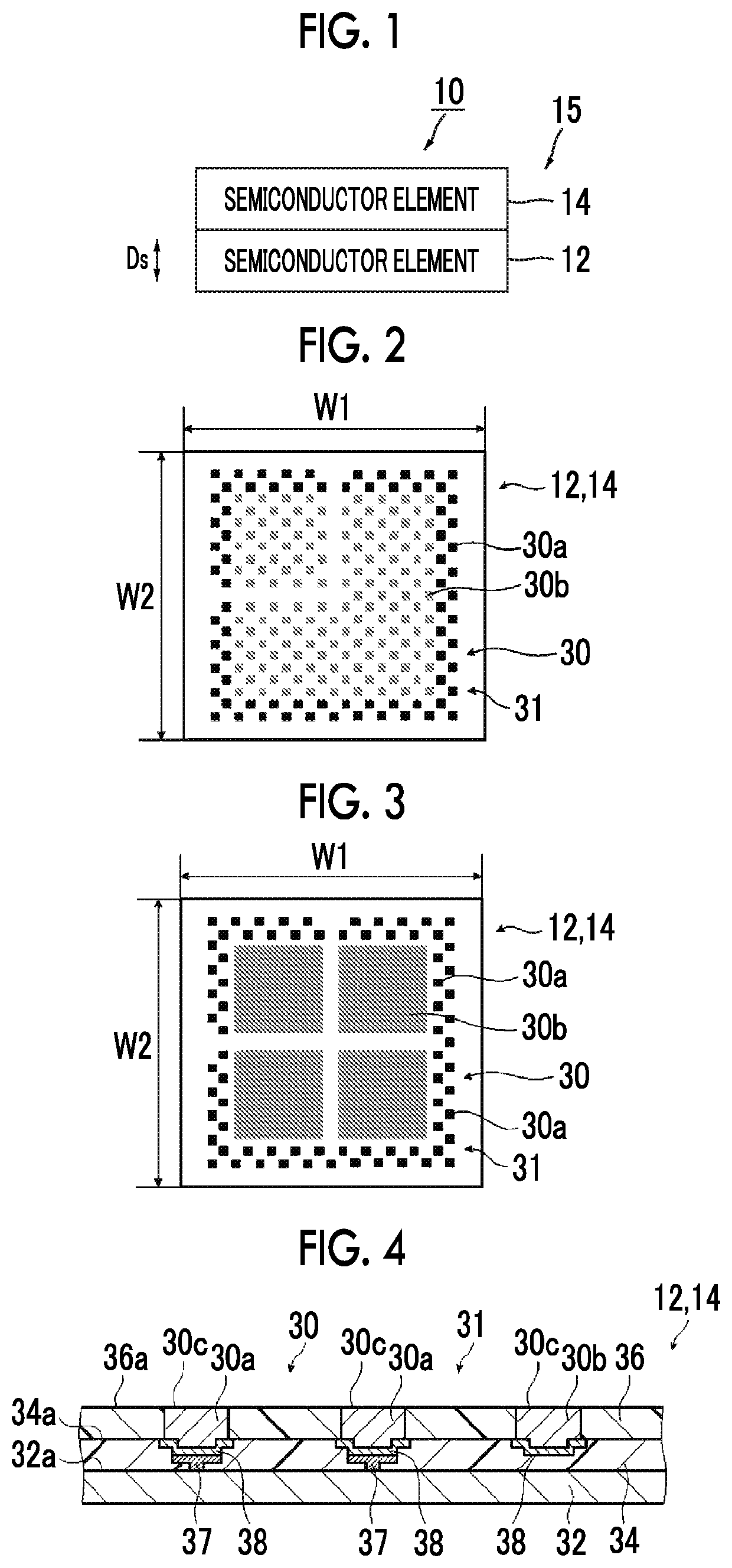
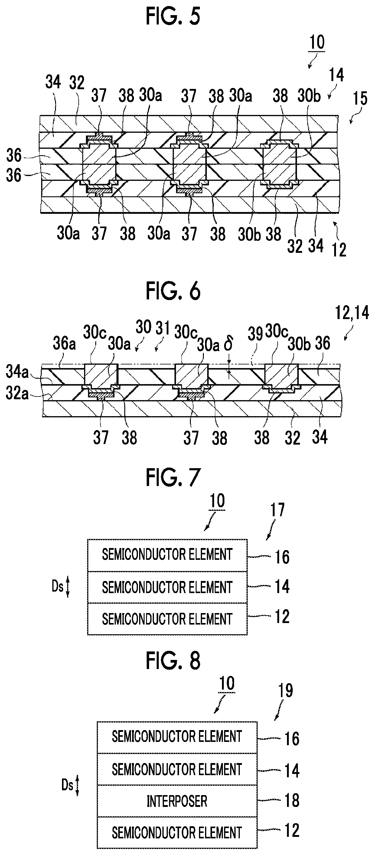
A stacked device includes a stacked structure in which a plurality of semiconductors are electrically connected to each other, the semiconductor includes a surface on which a plurality of terminals are provided, the plurality of terminals include a terminal that bonds and electrically connects the semiconductors to each other and a terminal that bonds the semiconductors to each other and does not electrically connect the semiconductors to each other, an area ratio of the plurality of terminals on the surface of the semiconductor is 40% or higher, and an area ratio of the terminals that bond and electrically connect the semiconductors to each other among the plurality of terminals is lower than 50%.

Description

CROSS-REFERENCE TO RELATED APPLICATIONS[0001]This application is a Continuation of PCT International Application No. PCT / JP2018 / 008902 filed on Mar. 8, 2018, which claims priority under 35 U.S.C. § 119(a) to Japanese Patent Application No. 2017-054444 filed on Mar. 21, 2017 and Japanese Patent Application No. 2017-170074 filed on Sep. 5, 2017. Each of the above application(s) is hereby expressly incorporated by reference, in its entirety, into the present application.BACKGROUND OF THE INVENTION1. Field of the Invention[0002]The present invention relates to a stacked device in which a plurality of semiconductor elements or the like are stacked, a stacked structure, and a method of manufacturing the stacked device. In particular, the present invention relates to a stacked device including a terminal that is electrically connected to a semiconductor element or the like and a terminal that is not electrically connected to a semiconductor element or the like, a stacked structure, and a m...

Claims


Application Information

Patent Timeline
IPC IPC(8): H01L25/065H01L23/00H01L25/00
CPCH01L25/0657H01L2224/32148H01L24/32H01L25/50H01L2225/06513H01L2225/06572H01L2225/06589H01L2225/06517H01L2224/94H01L2224/97H01L2225/06593H01L2924/3511H01L2924/37001H01L2224/08145H01L2224/0603H01L2224/06134H01L2224/16145H01L2224/131H01L2224/0401H01L2224/05624H01L2224/05647H01L2224/05567H01L2224/08225H01L2224/16227H01L2224/06519H01L24/06H01L2224/32145H01L2224/29078H01L2224/29076H01L2224/83851H01L2224/27002H01L2224/33181H01L2924/1431H01L2224/8013H01L2224/80132H01L2224/8113H01L2224/81132H01L2224/80013H01L2224/8009H01L2224/80075H01L2224/80205H01L2224/8313H01L2224/83132H01L2224/83075H01L2224/8309H01L2224/83013H01L2224/80097H01L2224/83191H01L2224/83907H01L2224/80907H01L24/29H01L24/80H01L24/83H01L2224/83005H01L2924/351H01L24/94H01L24/97H01L24/33H01L2224/09517H01L2224/80895H01L2224/80896H01L2224/80357H01L2224/8034H01L2224/83H01L2924/014H01L2924/00014H01L2924/013H01L2224/80H01L2224/81H01L23/528H01L23/485
Inventor HOTTA, YOSHINORI
Owner FUJIFILM CORP
Why Eureka
Try Eureka