Supercharge Your Innovation With Domain-Expert AI Agents!

Formation of air gap spacers for reducing parasitic capacitance

a technology of air gap spacer and capacitance reduction, which is applied in the direction of semiconductor devices, semiconductor/solid-state device details, electrical apparatus, etc., can solve the problems of resistor-capacitor delay time and device operating speed decrease, and achieve the effect of reducing parasitic capacitan

Active Publication Date: 2019-12-12
IBM CORP
View PDF16 Cites 28 Cited by
  • Summary
  • Abstract
  • Description
  • Claims
  • Application Information

AI Technical Summary

Benefits of technology

The patent text describes methods for reducing parasitic capacitance in semiconductor devices. The technical effects of these methods include improved performance and reliability of semiconductor devices, reduced power consumption, and reduced noise. The methods involve replacing a sacrificial layer with a gate structure, depositing and removing layers, and depositing a conductive material to form air gap spacers between the gate structure and the source and drain regions. These air gap spacers help to reduce parasitic capacitance and improve the performance and reliability of semiconductor devices.

Problems solved by technology

A consequence of having multiple layers of conductive structure separated by a dielectric material, however, is the formation of a parasitic capacitor between a transistor gate and a source / drain region.
The parasitic capacitance between the conductive material separated by the insulating material in microelectronic devices contributes to effects such as the resistor-capacitor (RC) delay time and a decrease of the device operating speed.

Method used


Image

  • Formation of air gap spacers for reducing parasitic capacitance
  • Formation of air gap spacers for reducing parasitic capacitance
  • Formation of air gap spacers for reducing parasitic capacitance

Examples


Embodiment Construction

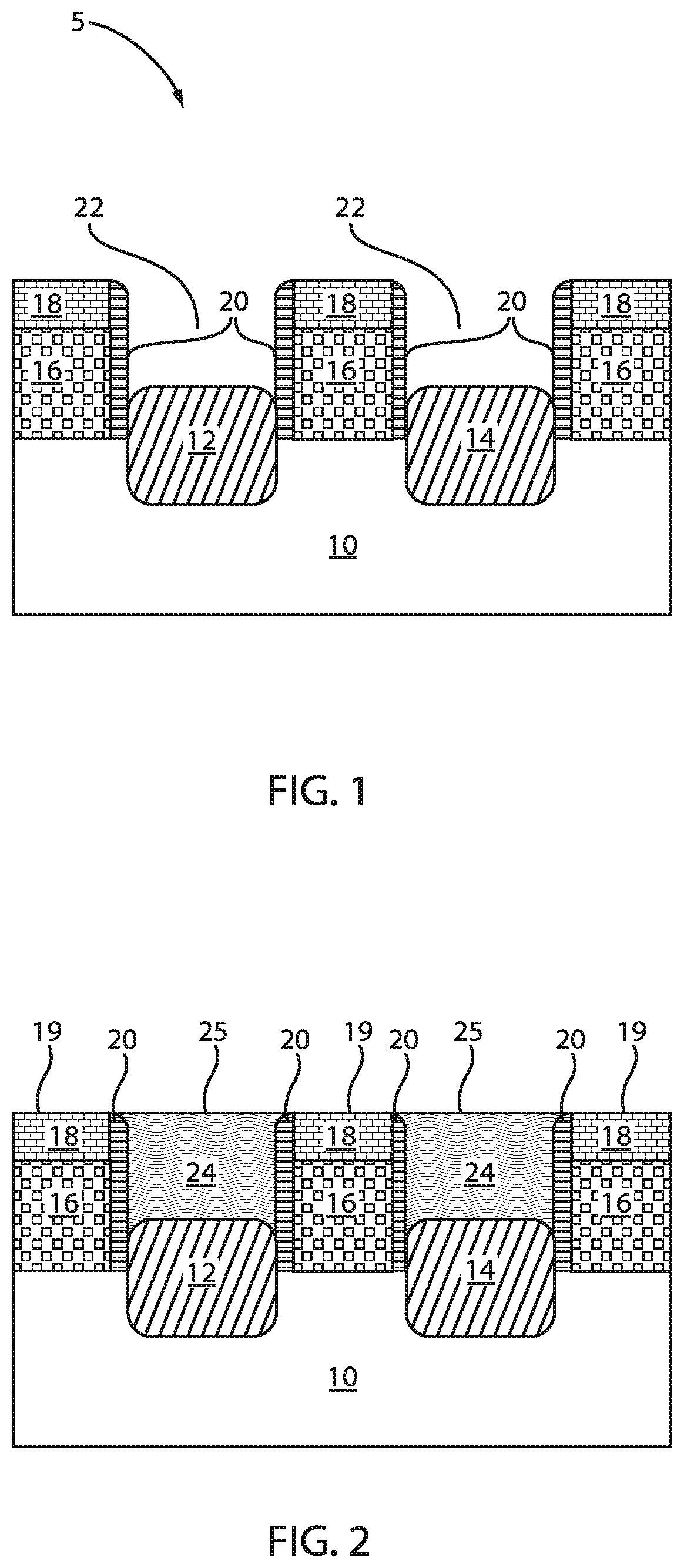
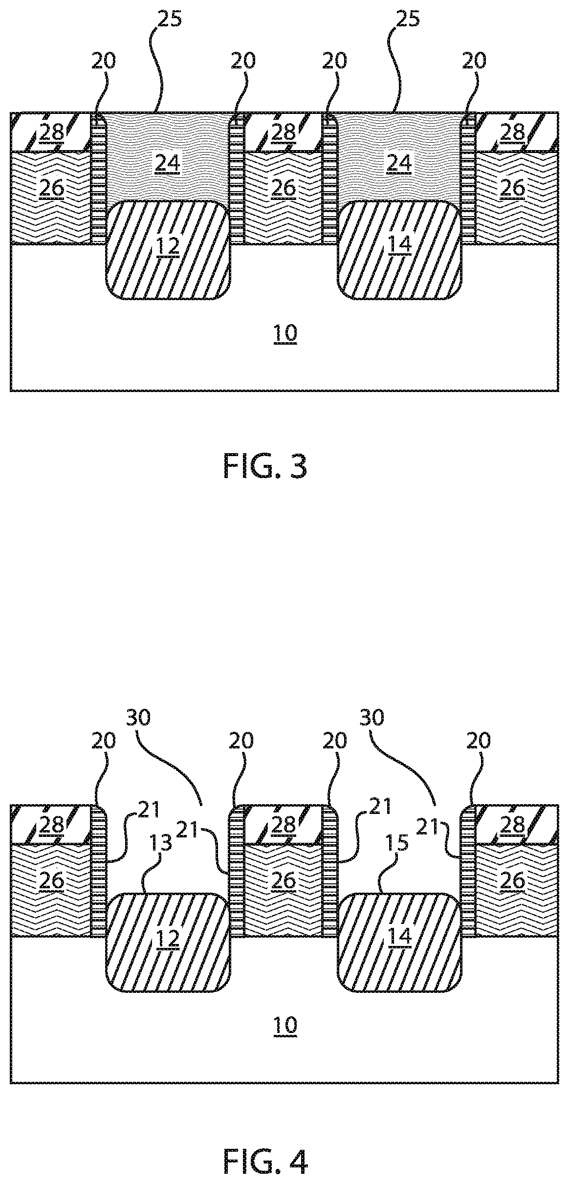
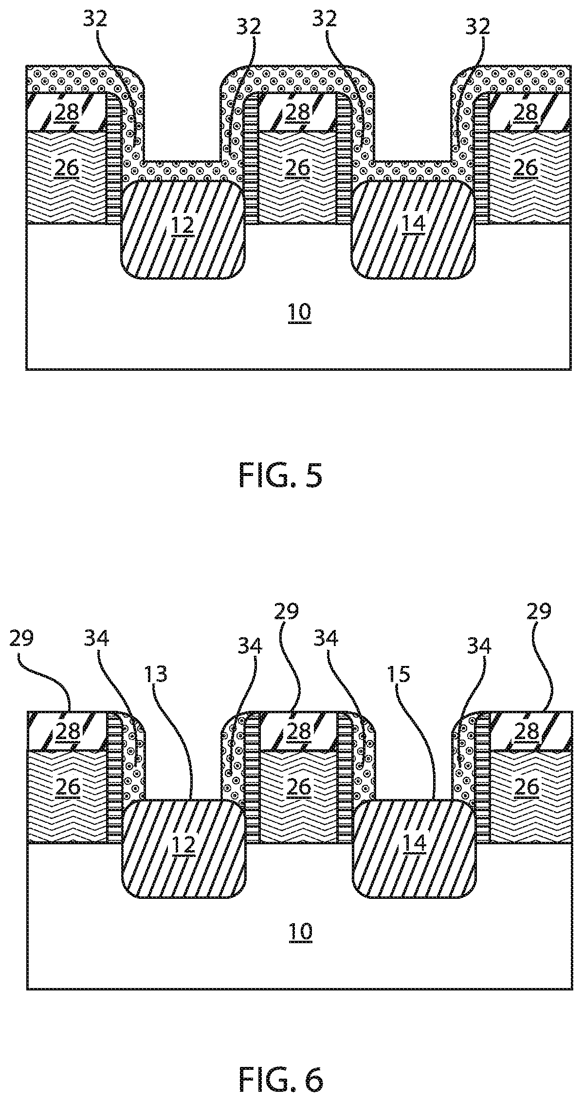
[0028]Embodiments in accordance with the present invention provide methods and devices for reducing parasitic capacitance between, e.g., gate structures and source / drain regions. In electrical circuits, parasitic capacitance is unwanted capacitance that exists between parts of an electronic component or circuit simply because of their proximity to each other. When two electrical conductors at different voltages are close together, the electric field between them causes electric charge to be stored thereon, which is referred to as parasitic capacitance. Therefore, reducing front end of line (FEOL) parasitic capacitance remains a focus for advanced technology node development. The exemplary embodiments provide for air-gaps that can be created and incorporated into semiconductor manufacturing technology to reduce parasitic capacitance.

[0029]Embodiments in accordance with the present invention provide methods and devices for forming air-gap spacers. The air-gap spacers can be formed by ...


PUM


Abstract

A method is presented for reducing parasitic capacitance. The method includes forming a source region and a drain region within a substrate, forming spacers in direct contact with sidewalls of a sacrificial layer, depositing an inter-layer dielectric (ILD) over the source and drain regions, replacing the sacrificial layer with a gate structure, removing the ILD, and depositing a sacrificial dielectric layer. The method further includes removing portions of the sacrificial dielectric layer to expose top surfaces of the source and drain regions, depositing a conductive material over the exposed top surfaces of the source and drain regions, and removing remaining portions of the sacrificial dielectric layer to form air gap spacers between the gate structure and the source and drain regions.

Description

BACKGROUNDTechnical Field[0001]The present invention relates generally to semiconductor devices, and more specifically, to forming air gap spacers to reduce parasitic capacitance.Description of the Related Art[0002]In the current fabrication of an integrated circuit, a dielectric layer is formed as a device isolation structure to cover a substrate and a transistor after completion of the manufacturing of the transistor. A consequence of having multiple layers of conductive structure separated by a dielectric material, however, is the formation of a parasitic capacitor between a transistor gate and a source / drain region. The parasitic capacitance between the conductive material separated by the insulating material in microelectronic devices contributes to effects such as the resistor-capacitor (RC) delay time and a decrease of the device operating speed.SUMMARY[0003]In accordance with an embodiment, a method is provided for reducing parasitic capacitance. The method includes forming ...

Claims


Application Information

Patent Timeline
IPC IPC(8): H01L29/49H01L21/768H01L23/522H01L29/08H01L29/66
CPCH01L29/0847H01L23/5226H01L21/76829H01L29/4991H01L21/7682H01L29/6656H01L29/66545H01L29/6653H01L29/66795H01L29/785H01L21/76897H01L2221/1063
Inventor CHENG, KANGGUOXU, PENGLEE, CHOONGHYUNWU, HENG
Owner IBM CORP
Features
  • R&D
  • Intellectual Property
  • Life Sciences
  • Materials
  • Tech Scout
  • Unparalleled Data Quality
  • Higher Quality Content
  • 60% Fewer Hallucinations
Learn More