Wiring substrate and display device including the same

Active Publication Date: 2020-01-02
SAMSUNG DISPLAY CO LTD
View PDF0 Cites 2 Cited by
  • Summary
  • Abstract
  • Description
  • Claims
  • Application Information

AI Technical Summary

Benefits of technology

This patent is about a display device that can prevent the thin film transistor from getting damaged. It also mentions a wiring substrate that can prevent the thin film transistor from getting damaged.

Problems solved by technology

However, when a high source-drain voltage is applied to the thin film transistor, the operational characteristics of the thin film transistor may deteriorate, which may affect the durability and reliability of a display device.

Method used


Image

  • Wiring substrate and display device including the same
  • Wiring substrate and display device including the same
  • Wiring substrate and display device including the same

Examples


preparation example 1

[0142]As shown in FIG. 9, a thin film transistor including a gate pattern, a semiconductor pattern, a source pattern, and a drain pattern was prepared. The gate pattern had a double-layered structure of a titanium pattern layer and a copper pattern layer, and the copper pattern layer had a thickness of about 2,000 Å. The semiconductor pattern included indium-gallium-zinc oxide (IGZO). The semiconductor pattern had a thickness of about 500 Å. Each of the source pattern and the drain pattern had a double-layered structure of a molybdenum pattern layer and a copper pattern layer, and the molybdenum pattern layer had a thickness of about 500 Å.

[0143]The distance (that is, channel length) between the source pattern and the drain pattern, measured along the direction of current flow, was 5.5 μm. The overlap length (that is, overlap length of drain pattern) of the drain pattern, the semiconductor pattern, and the gate pattern, measured along the direction of current flow, was 4.5 μm. The w...

preparation example 2

[0144]A thin film transistor was prepared in the same manner as in Preparation Example 1, except that the channel length was changed to 4.5 μm.

experimental example 1

[0149]The drain current retention rates of the thin film transistors according to Preparation Example 1 and Preparation Example 2 were measured, and the results thereof are shown in FIG. 13. Further, the drain current (ID) characteristics of the thin film transistors according to Preparation Example 1 and Preparation Example 2 vs. the gate-source voltage (VGS) are shown in FIGS. 16 and 17, respectively. The drain current retention rate of the thin film transistor according to Preparation Example 1 was about 96.4%, and the drain current retention rate of the thin film transistor according to Preparation Example 2 was about 57.1%.

[0150]After a voltage of 20 V was applied to the gate pattern of the thin film transistor and a voltage of 65 V was applied to the source pattern of the thin film transistor, an initial drain current (ID0) was measured. Further, after the voltages were applied to the gate pattern and the source pattern for 1 hour, respectively, a drain current (ID) was measur...


PUM


Abstract

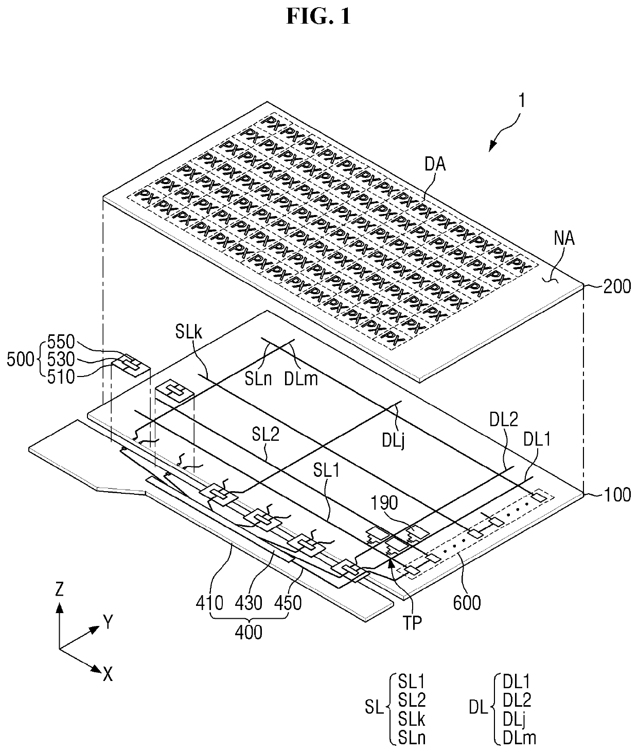
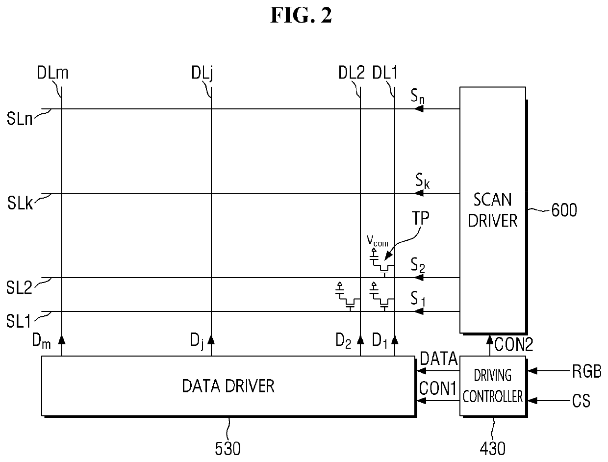
A display device in which a display area and a non-display area are defined, the display device including a wiring substrate, the wiring substrate including: a base substrate; a first thin film transistor disposed on the base substrate, located in the non-display area, and including a first gate pattern, a first semiconductor pattern disposed on the first gate pattern, a first source pattern disposed on the first semiconductor pattern, and a first drain pattern disposed on the first semiconductor pattern and spaced apart from the first source pattern; and a second thin film transistor disposed on the base substrate and located in the display area. A first channel width of the first thin film transistor is greater than a first overlap length of the first gate pattern, the first semiconductor pattern, and the first drain pattern.

Description

CROSS REFERENCE TO RELATED APPLICATION[0001]This application claims priority from and the benefit of Korean Patent Application No. 10-2018-0074948, filed on Jun. 28, 2018, which is hereby incorporated by reference for all purposes as if fully set forth herein.BACKGROUNDField[0002]Exemplary embodiments of the invention relate generally to a wiring substrate and a display device including the wiring substrate.Discussion of the Background[0003]The importance of a display device has increased with the development of multimedia. Accordingly, various types of display devices, such as a liquid crystal display (LCD), an organic light emitting diode display (OLED) and the like have been developed.[0004]One of the driving methods of the liquid crystal display device or the organic light emitting display device is an active matrix driving method. The active matrix driving method has an advantage in that each pixel can be driven individually, as compared with a passive matrix driving method in ...

Claims


Application Information

Patent Timeline
IPC IPC(8): H01L27/12H01L29/786G09G3/36
CPCG09G3/3696H01L27/124H01L29/78696H01L29/78618H01L27/1218H01L27/1225H01L29/41733H01L29/7869G02F1/1368G02F1/136286H01L27/1214
Inventor MOON, YEON KEONMASATAKA, KANOKIM, MYOUNG HWALIM, JUN HYUNG
Owner SAMSUNG DISPLAY CO LTD
Why Eureka
Try Eureka