Semiconductor device

Active Publication Date: 2020-01-16
FUJI ELECTRIC CO LTD
View PDF0 Cites 6 Cited by
  • Summary
  • Abstract
  • Description
  • Claims
  • Application Information

AI Technical Summary

Benefits of technology

The patent describes a circuit that uses a diode to protect a certain component from overvoltage. This circuit helps to prevent damage to the electronic device caused by high voltages.

Problems solved by technology

Further, the rate of temperature increase corresponding to the unit-cell occupied volume increases the extent to which the current density of the device is increased and a problem such as peeling of bonding wires occurs, necessitating a double-sided cooling structure to achieve improvements in discharge rate and stabilizing reliability.

Method used


Image

  • Semiconductor device
  • Semiconductor device
  • Semiconductor device

Examples


Embodiment Construction

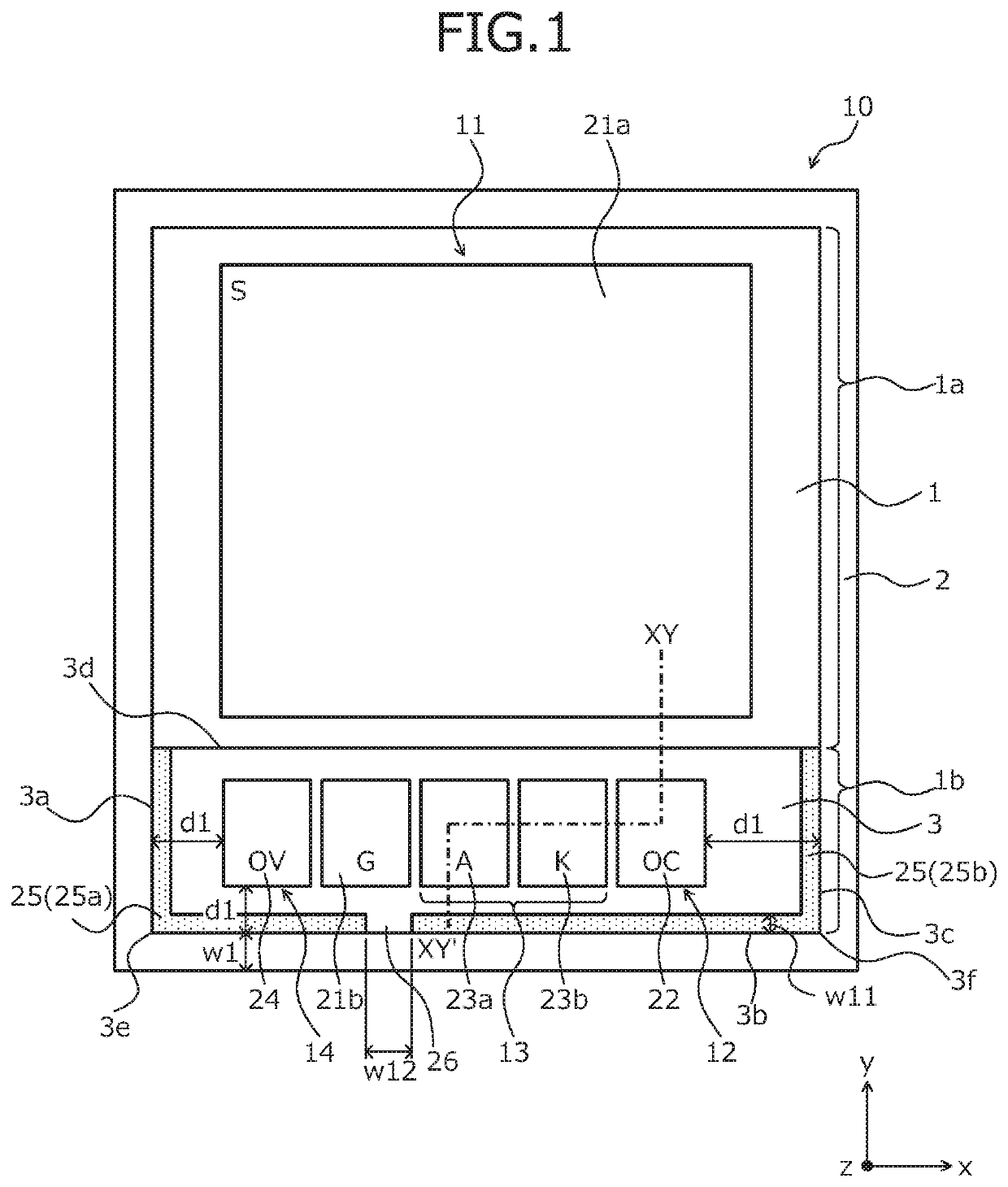
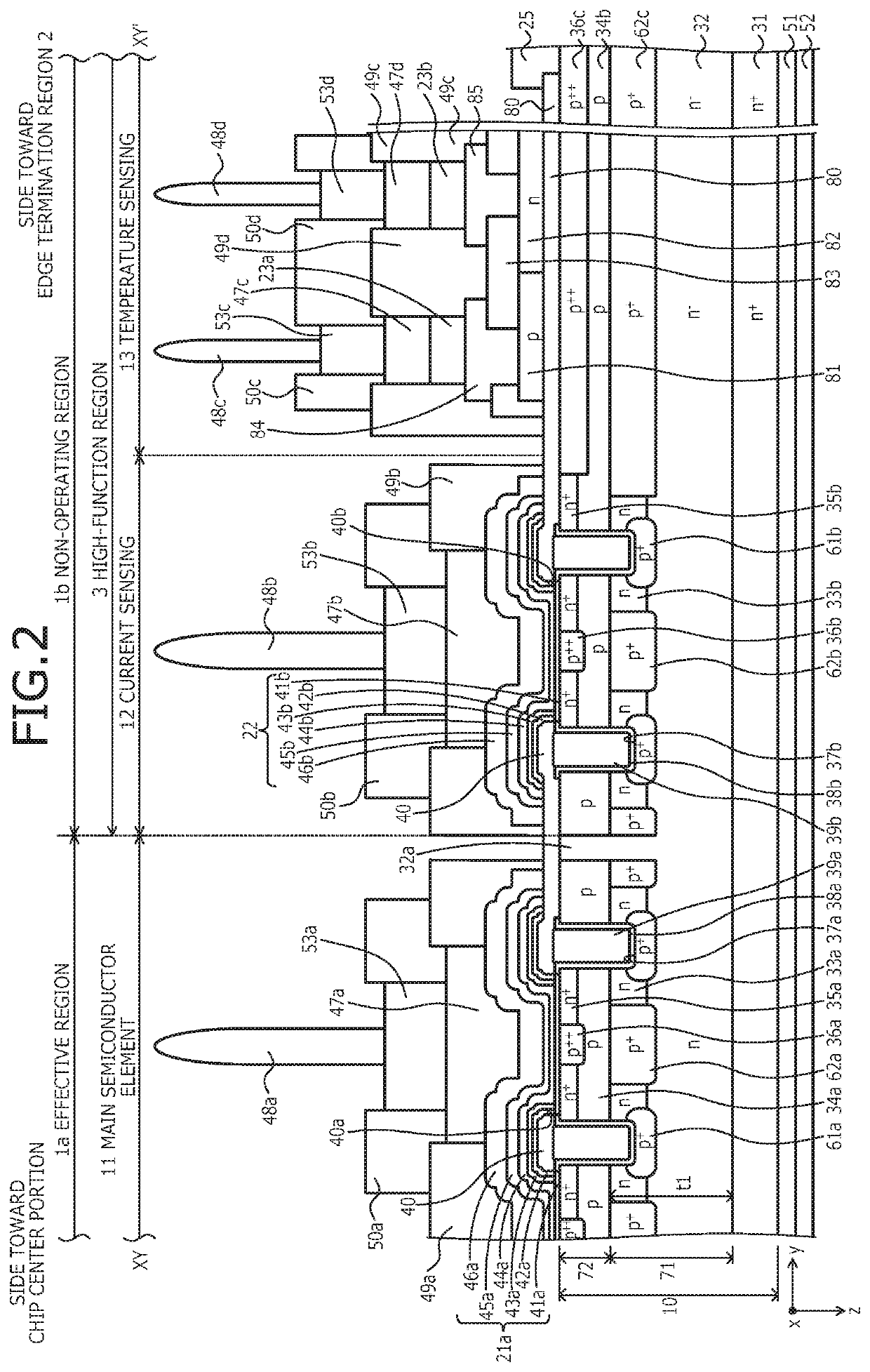
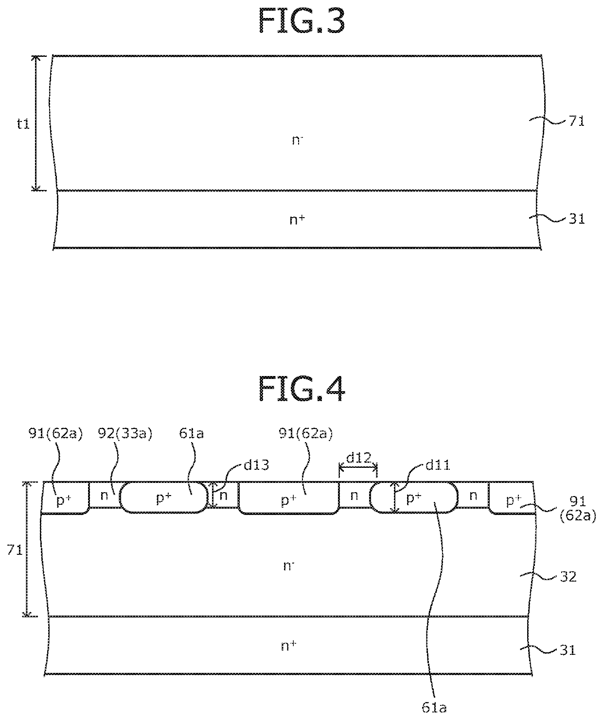
[0031]First, problems associated with the conventional techniques will be discussed. In the conventional semiconductor device (refer to FIG. 11) described, a wide bandgap semiconductor material is used as a semiconductor material and therefore, as compared to a case in which silicon is used as a semiconductor material, a width w101 of the edge termination region 102 may be reduced by about ⅕ to ½. Additionally, a thickness (thickness of the semiconductor substrate 110) of the edge termination region 102 may be reduced by ½. Therefore, the width w101 of the edge termination region 102 is reduced and the thickness of the edge termination region 102 is reduced, thereby enabling ON resistance (RonA) of the MOSFET 111 to be reduced.

[0032]Nonetheless, by reducing the width w101 of the edge termination region 102 and the thickness of the edge termination region 102, capacitance (pn junction capacitance) of a depletion layer that in a direction (horizontal direction) parallel to the front s...


PUM


Abstract

In an effective region of an active region, a main semiconductor element and a source pad thereof are disposed. A non-operating region of the active region excludes the effective region and is a high-function region in which a gate pad of the main semiconductor element and other electrode pads are disposed. An edge termination region and the electrode pads are separated by an interval equivalent to at least a width of one unit cell of the main semiconductor element. In the high-function region, at a border of the edge termination region, a lead-out electrode is provided on a front surface of a semiconductor substrate. The lead-out electrode has a function of leading out displacement current that flows to the high-function region from the edge termination region when the main semiconductor element is OFF. Thus, destruction at the edge termination region may be suppressed.

Description

CROSS REFERENCE TO RELATED APPLICATIONS[0001]This is a continuation application of International Application PCT / JP2018 / 031240 filed on Aug. 23, 2018 which claims priority from a Japanese Patent Application No. 2017-195431 filed on Oct. 5, 2017, the contents of which are incorporated herein by reference.BACKGROUND OF THE INVENTION1. Field of the Invention[0002]Embodiments of the invention relate to a semiconductor device.2. Description of the Related Art[0003]Semiconductor materials (hereinafter, wide bandgap semiconductor materials) having a bandgap that is wider than that of silicon (Si) are gaining attention as a semiconductor material enabling fabrication (manufacture) of next generation power semiconductor devices having excellent high-temperature characteristics, high-speed characteristics, and low ON voltage. Further, conventionally, in a power semiconductor device that uses a wide bandgap semiconductor material, a trench gate structure is adopted in a vertical metal oxide se...

Claims


Application Information

Patent Timeline
IPC IPC(8): H01L29/78H01L21/8234H01L27/06H01L29/49H01L29/06H01L29/16H01L29/10H01L29/08
CPCH01L29/7811H01L21/8234H01L29/0692H01L29/4941H01L29/0878H01L29/1608H01L29/1095H01L27/06H01L21/8213H01L21/823481H01L27/0629H01L29/0623H01L29/66068H01L29/7813H01L29/7815H01L2224/0603
Inventor SUZUKI, YOSHIHISAKUMADA, KEISHIROUHOSHI, YASUYUKIHASHIZUME, YUICHI
Owner FUJI ELECTRIC CO LTD
Why Eureka
Try Eureka