Organic el image display device
an image display device and organic technology, applied in the direction of optical elements, identification means, instruments, etc., can solve the problems of image blurring, and achieve the effects of reducing image blurring, high brightness, and reducing image blurring
- Summary
- Abstract
- Description
- Claims
- Application Information
AI Technical Summary
Benefits of technology
Problems solved by technology
Method used
Image
Examples
example 1
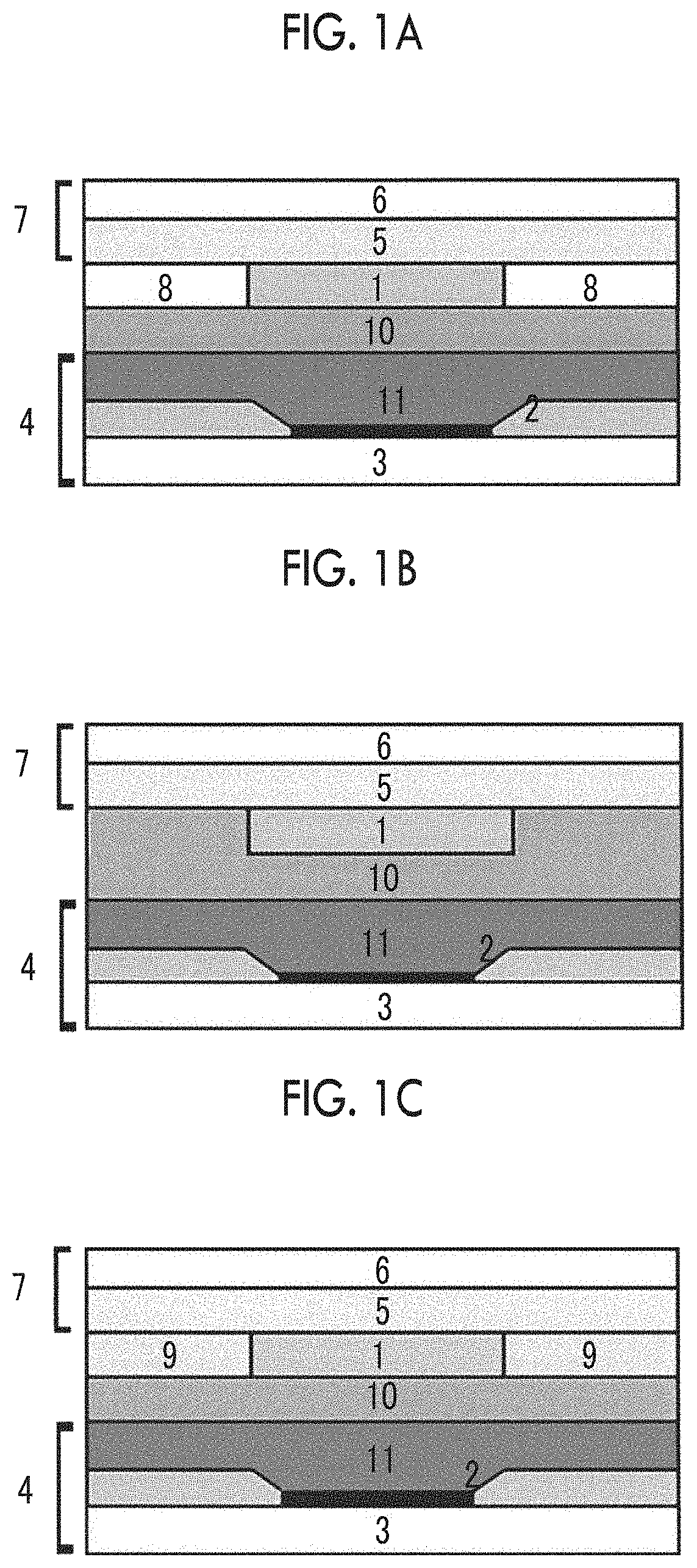
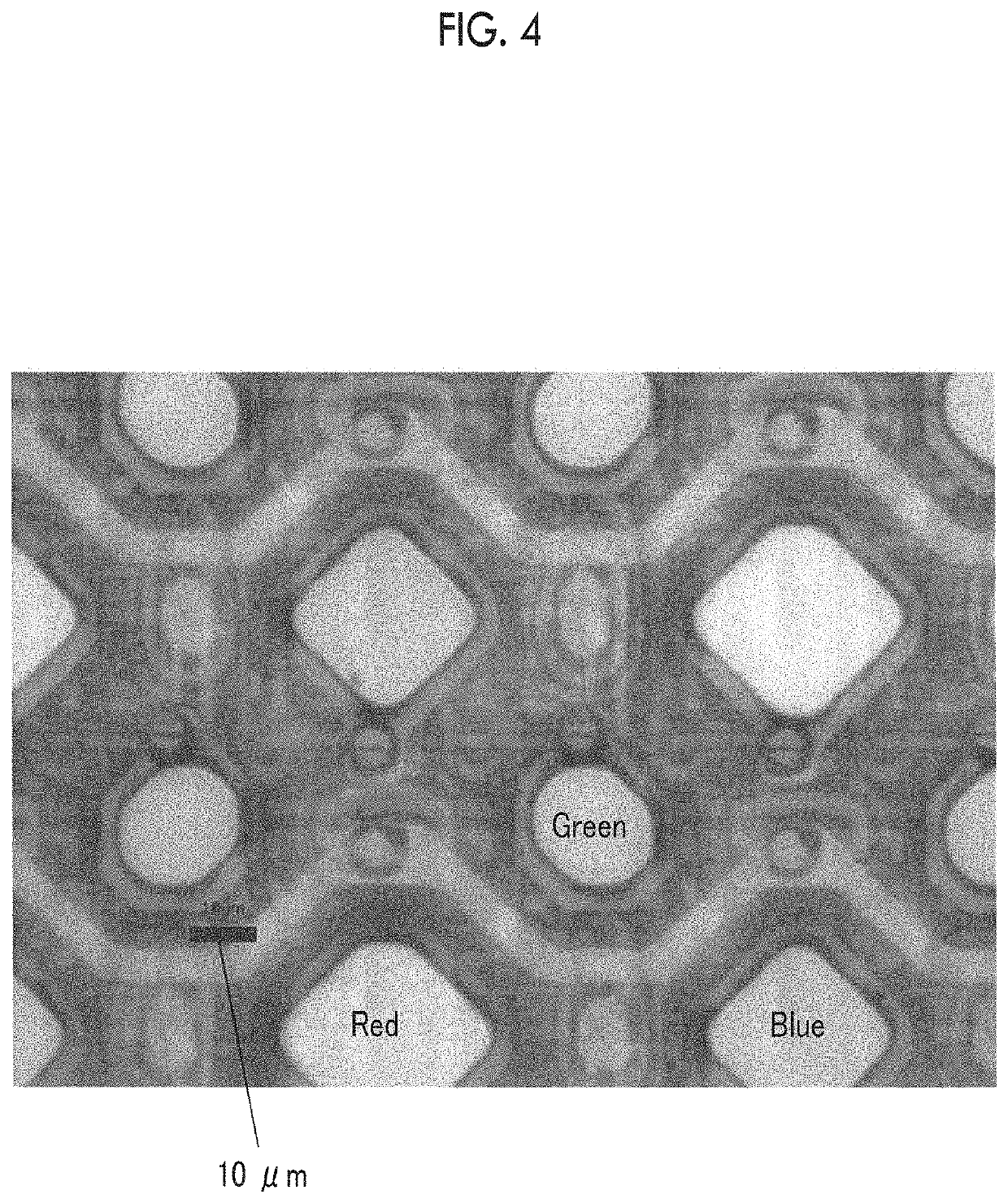
[0231]The alignment film composition A was uniformly applied to a glass substrate using a slit coater, and then dried for 2 minutes in an oven at 100° C. to obtain a glass substrate with an alignment film having a thickness of 0.5 μm. The alignment film was rubbed in a direction parallel to the coating direction. The liquid crystal composition LC-1 was applied to the rubbed surface. Next, the composition was heated and aged at a film surface temperature of 95° C. for 60 seconds, and immediately thereafter, the composition was exposed via a photo mask A shown in FIG. 3 (value of b: 57.7 μm: value of b corresponding to L of Expression (1)) at an exposure dose of 100 mJ / cm2 using a PLA-501F exposure machine (super high pressure mercury lamp) manufactured by Canon Inc. under air at 25° C. In FIG. 3, white refers to a transmission part and black refers to a shielding part. Then, by exposing the entire substrate to light under nitrogen by an air-cooled metal halide lamp (manufactured by E...
example 2
[0234]A layer having the cholesteric liquid crystal layer pattern was prepared in the same manner as in Example 1 except that a photo mask B, in which the value of b in FIG. 3 was set to 30.00 μm, was used during pattern formation. Furthermore, a layer having the cholesteric liquid crystal layer pattern and a circularly polarizing plate CP1 are laminated in the same manner as in Example 1 on the barrier layer surface of the light emitting element substrate prepared in the same manner as in Example 1 to prepare the image display device for evaluation.
example 3
[0235]A layer having the cholesteric liquid crystal layer pattern was prepared in the same manner as in Example 1 except that a photo mask C, in which the value of b in FIG. 3 was set to 20.00 μm, was used during pattern formation. Furthermore, a layer having the cholesteric liquid crystal layer pattern and a circularly polarizing plate CP1 were laminated in the same order as in Example 1 on the barrier layer surface of the light emitting element substrate prepared in the same manner as in Example 1 to prepare the image display device for evaluation.
PUM
 Abstract
Description
Claims
Application Information


