
Gallium nitride substrate

a technology of gallium nitride and substrate, which is applied in the direction of single crystal growth details, single crystal growth, chemistry apparatus and processes, etc., can solve the problem of multiple crystal defects in the gan crystal, and achieve the effect of suppressing cracks and breakag

Active Publication Date: 2020-01-30
SUMITOMO ELECTRIC IND LTD
View PDF0 Cites 0 Cited by
  • Summary
  • Abstract
  • Description
  • Claims
  • Application Information

AI Technical Summary

Benefits of technology

The patent explains a way to prevent cracks and breaks when another semiconductor layer is being grown epitaxially.

Problems solved by technology

Since lattice constant and thermal expansion coefficient are different between the heterogeneous substrate and the GaN crystal, a multiplicity of crystal defects are generated in the GaN crystal, disadvantageously.

Method used


Image

  • Gallium nitride substrate
  • Gallium nitride substrate
  • Gallium nitride substrate

Examples


first embodiment

GaN Substrate

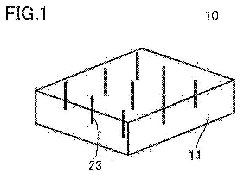
[0025]FIG. 1 shows a schematic perspective view of a portion of a surface of a GaN substrate of a first embodiment. A GaN substrate 10 of the first embodiment is composed of a GaN crystal 11. Regions having threading dislocations 23 intensively located therein are formed to extend from a surface of GaN crystal 11 toward inside of GaN crystal 11.

Method for Manufacturing GaN Substrate

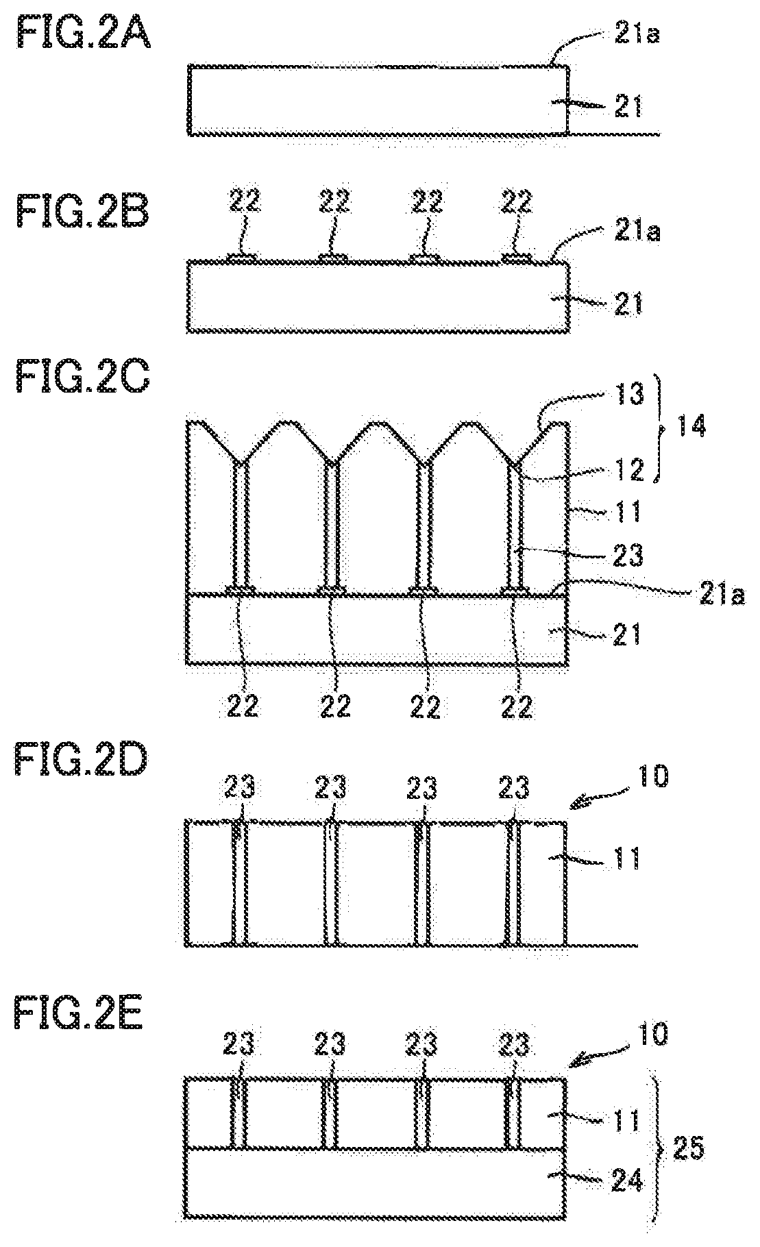
[0026]With reference to schematic cross sectional views of FIG. 2A to FIG. 2D, the following describes an exemplary method for manufacturing the GaN substrate of the first embodiment. First, as shown in FIG. 2A, a growth substrate 21 is prepared which has a surface 21a to serve as a growth surface. Growth substrate 21 is not particularly limited as long as GaN crystal 11 can be grown on surface 21a. Examples of growth substrate 21 may include: a heterogeneous substrate such as gallium arsenide (GaAs); and a homogeneous substrate composed of GaN.

[0027]Next, as shown in FIG. 2B, a patterning la...

second embodiment

[0057]A feature of a GaN substrate 10 of a second embodiment lies in that it is different from the first embodiment in the following points (i) to (iii).

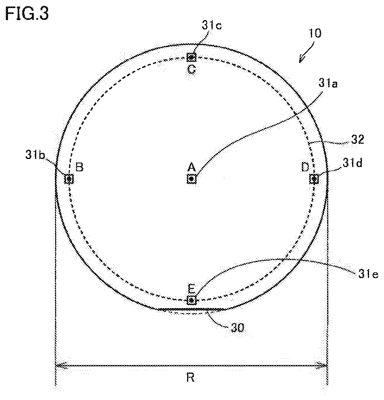
[0058](i) GaN substrate 10 has a surface having a diameter R of not less than 150 mm.

[0059](ii) A difference (Δkp (2 mm□)) is not less than 0.1 cm−1 and not more than 1 cm−1 between maximum and minimum values of Raman shift amounts corresponding to the E2H phonon mode in Raman spectra obtained through micro-Raman scattering mapping measurement in each of square regions 31a, 31b, 31c, 31d, 31e having sides each having a length of 2 mm, the square regions having respective centers at a total of five points including a central point A and circumferential edge points B, C, D and E on the surface of GaN substrate 10.

[0060](iii) A difference (Δkp (entire surface)) is not more than 1 cm−1 between maximum and minimum values of the Raman shift amounts corresponding to the E2H phonon mode in the Raman spectra at all of the measurement points ...

third embodiment

[0063]A feature of a GaN substrate 10 of a third embodiment lies in that a square region having sides each having a length of 2 mm on a surface of GaN substrate 10 include: a region having a threading dislocation density of not less than 1×106 cm−2; and a region having a threading dislocation density of less than 1×106 cm−2. In GaN substrate 10 of the third embodiment, dislocations are located intensively in a region (core portion 12) having a threading dislocation density of not less than 1×106 cm−2, thereby improving crystallinity of the region (facet 13) having a threading dislocation density of less than 1×106 cm−2.

[0064]Each square region having sides each having a length of 2 mm on the surface of GaN substrate 10 includes the region having a threading dislocation density of not less than 1×106 cm−2 and the region having a threading dislocation density of less than 1×106 cm−2 as in the third embodiment presumably because the following phenomena (I) to (V) occur in this order in...


PUM

PropertyMeasurementUnit
diameteraaaaaaaaaa
diameteraaaaaaaaaa
threading dislocation densityaaaaaaaaaa

Abstract

A gallium nitride substrate has a surface with a diameter of not less than 100 mm, a difference being not less than 0.1 cm−1 and not more than 2 cm−1 between maximum and minimum values of wave numbers at a maximum peak of peaks corresponding to an E2H phonon mode in micro-Raman scattering mapping measurement at each of square regions having sides each having a length of 2 mm, the square regions being located at a total of five locations including a central location and four circumferential edge locations on the surface of the gallium nitride substrate, a difference being not more than 2 cm−1 between maximum and minimum values of the wave numbers at the maximum peak of the peaks corresponding to the E2H phonon mode at all of measurement points in the five locations.

Description

TECHNICAL FIELD[0001]The present invention relates to a gallium nitride (GaN) substrate.BACKGROUND ART[0002]Among nitride semiconductor substrates, GaN substrates have been drawing attention as substrates for manufacturing semiconductor devices such as a light emitting device and an electronic device. However, at present, for manufacturing of a GaN substrate, growth has to be performed on a heterogeneous substrate. Since lattice constant and thermal expansion coefficient are different between the heterogeneous substrate and the GaN crystal, a multiplicity of crystal defects are generated in the GaN crystal, disadvantageously.[0003]To address this, for example, Non-Patent Document 1 discloses a GaN substrate, wherein a GaN crystal provided with a multiplicity of dot-shaped depressions in its surface is grown such that crystal defects are located intensively at the centers of the depressions in the GaN crystal and crystal defects are reduced around the depressions.CITATION LISTNon Pat...

Claims


Application Information

Patent Timeline
Patent Type & Authority Applications(United States)
IPC IPC(8): C30B29/40C30B25/02C30B29/64
CPCC30B29/406C30B25/02C30B29/64
Inventor KIYAMA, MAKOTOHIROTA, RYUNAKAHATA, SEIJI
Owner SUMITOMO ELECTRIC IND LTD
Learn More