
Gallium nitride substrate

a technology of gallium nitride and substrate, which is applied in the direction of single crystal growth, polycrystalline material growth, chemistry apparatus and processes, etc., can solve the problem of multiple crystal defects in the gan crystal, and achieve the effect of suppressing cracks and breakag

Active Publication Date: 2019-10-29
SUMITOMO ELECTRIC IND LTD
View PDF10 Cites 2 Cited by
  • Summary
  • Abstract
  • Description
  • Claims
  • Application Information

AI Technical Summary

Benefits of technology

[0009]According to the description above, occurrence of crack and breakage can be suppressed when epitaxially growing another semiconductor layer.

Problems solved by technology

Since lattice constant and thermal expansion coefficient are different between the heterogeneous substrate and the GaN crystal, a multiplicity of crystal defects are generated in the GaN crystal, disadvantageously.

Method used


Image

  • Gallium nitride substrate
  • Gallium nitride substrate
  • Gallium nitride substrate

Examples


experiment example 1

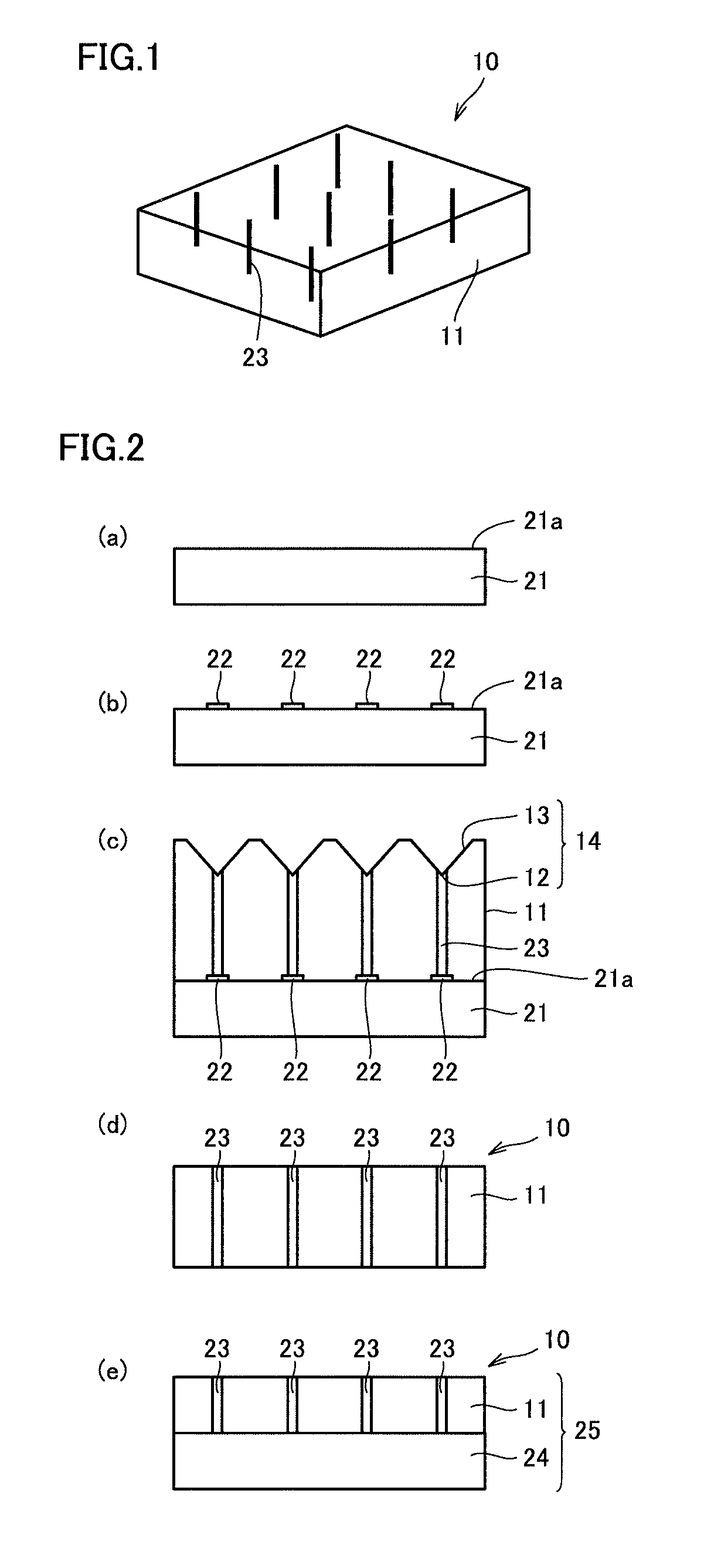
[0084]First, as shown in FIG. 2(a), as growth substrate 21, there was prepared a sapphire substrate having a surface (C plane) 21a having a diameter of 110 mm. Next, as shown in FIG. 2(b), a SiO2 film having a thickness of 0.1 μm was formed on the C plane of the sapphire substrate through plasma CVD, and then photolithography and etching employing BHF (buffered hydrofluoric acid) were performed to form a patterning layer 22 constituted of a SiO2 film. Patterning layer 22 had such a shape that circles each having a diameter of 50 μm were arranged in the form of a lattice at a pitch of 800 μm, and lattice directions were matched with an m-axis direction and an a-axis direction.

[0085]Next, as shown in FIG. 2(c), GaN crystal 11 was grown for 10 hours to have a thickness of about 1200 μm, on the C plane of the sapphire substrate having patterning layer 22 formed thereon and serving as growth substrate 21. GaN crystal 11 was grown through HVPE employing metallic Ga as a Ga source material...

experiment example 2

[0091]A C-plane GaN template substrate was used which had a surface having a diameter of 110 mm and had a GaN film having a thickness of 2 μm and formed through MOCVD on a sapphire substrate serving as growth substrate 21. A patterning layer 22 constituted of a SiO2 film was formed in the same manner as in experiment example 1. A GaN crystal was grown on patterning layer 22 by the same method and under the same conditions as those in experiment example 1 without forming a low-temperature GaN buffer layer. In this way, a GaN substrate of experiment example 2 was produced (with a finishing thickness of 500 μm), which was a freestanding GaN substrate having a circular shape with a diameter of 100 mm, having a C plane as a surface, and having a facet structure.

[0092]Then, in the same manner as in experiment example 1, a difference (Δkp (2 mm□)) was determined between maximum and minimum values of wave numbers at the maximum peak of peaks corresponding to the E2H phonon mode in the Raman...

experiment example 3

[0093]With the same method and under the same conditions as those in experiment example 1, a low-temperature GaN buffer layer is formed and a GaN crystal is grown on a GaAs substrate serving as growth substrate 21 and having a surface ((111) A plane) having a diameter of 110 mm. In this way, a GaN substrate of experiment example 3 was produced (with a finishing thickness of 500 μm), which was a freestanding GaN substrate having a circular shape with a diameter of 100 mm, having a C plane as a surface, and having a facet structure.

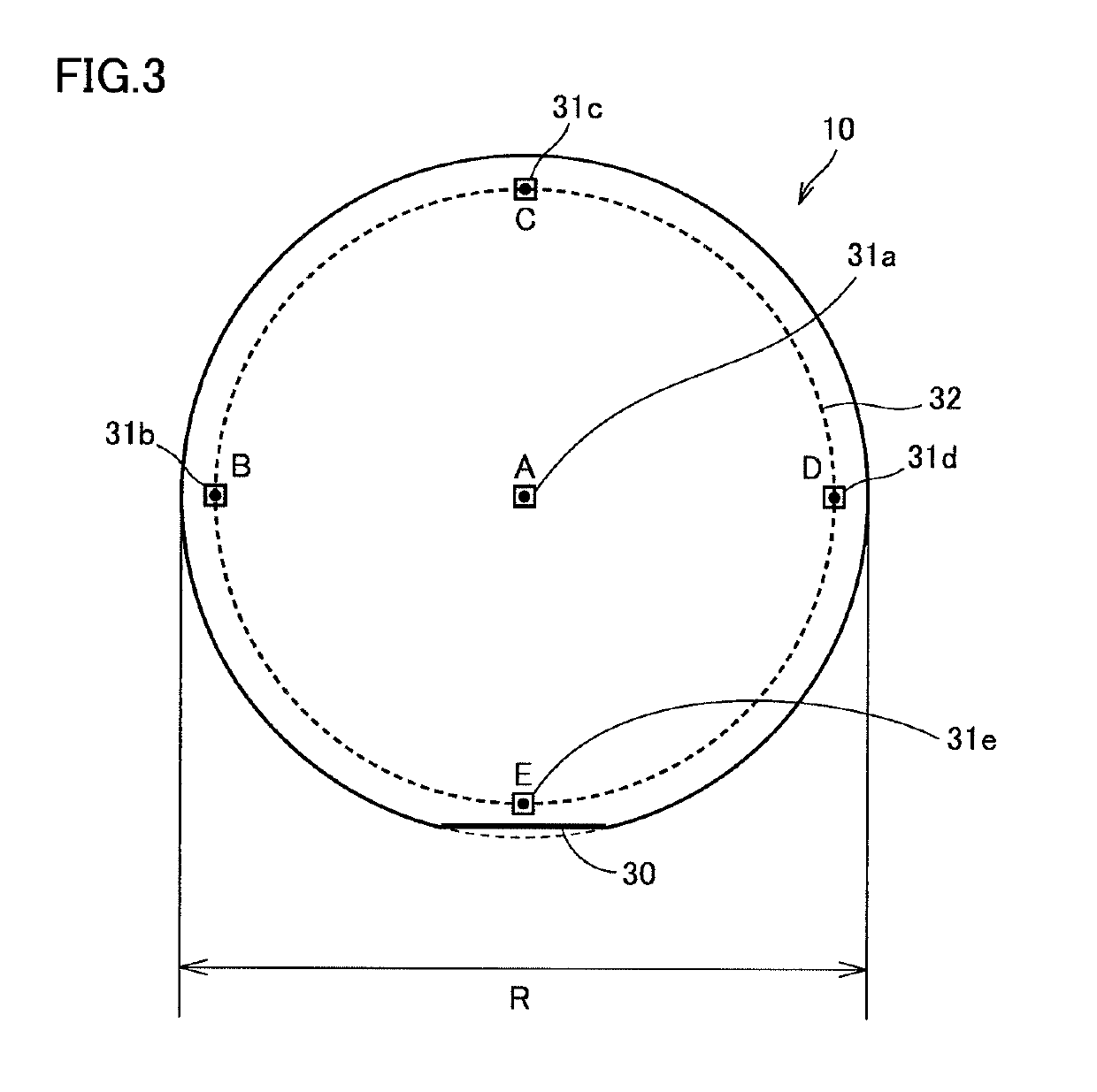
[0094]Then, in the same manner as in experiment example 1, a difference (Δkp (2 mm□)) was determined between maximum and minimum values of wave numbers at the maximum peak of peaks corresponding to the E2H phonon mode in the Raman spectra obtained through the micro-Raman scattering mapping measurement in each of square regions 31a, 31b, 31c, 31d, 31e having sides each having a length of 2 mm, the square regions having respective centers at a total of five p...


PUM

PropertyMeasurementUnit
diameteraaaaaaaaaa
lengthaaaaaaaaaa
diameteraaaaaaaaaa

Abstract

A gallium nitride substrate has a surface with a diameter of not less than 100 mm, a difference being not less than 0.1 cm−1 and not more than 2 cm−1 between maximum and minimum values of wave numbers at a maximum peak of peaks corresponding to an E2H phonon mode in micro-Raman scattering mapping measurement at each of square regions having sides each having a length of 2 mm, the square regions being located at a total of five locations including a central location and four circumferential edge locations on the surface of the gallium nitride substrate, a difference being not more than 2 cm−1 between maximum and minimum values of the wave numbers at the maximum peak of the peaks corresponding to the E2H phonon mode at all of measurement points in the five locations.

Description

TECHNICAL FIELD[0001]The present invention relates to a gallium nitride (GaN) substrate.BACKGROUND ART[0002]Among nitride semiconductor substrates, GaN substrates have been drawing attention as substrates for manufacturing semiconductor devices such as a light emitting device and an electronic device. However, at present, for manufacturing of a GaN substrate, growth has to be performed on a heterogeneous substrate. Since lattice constant and thermal expansion coefficient are different between the heterogeneous substrate and the GaN crystal, a multiplicity of crystal defects are generated in the GaN crystal, disadvantageously.[0003]To address this, for example, Non-Patent Document 1 discloses a GaN substrate, wherein a GaN crystal provided with a multiplicity of dot-shaped depressions in its surface is grown such that crystal defects are located intensively at the centers of the depressions in the GaN crystal and crystal defects are reduced around the depressions.CITATION LISTNon Pat...

Claims


Application Information

Patent Timeline
Patent Type & Authority Patents(United States)
IPC IPC(8): B32B9/00C30B25/02C30B29/64C30B29/40
CPCC30B29/64C30B29/406C30B25/02
Inventor KIYAMA, MAKOTOHIROTA, RYUNAKAHATA, SEIJI
Owner SUMITOMO ELECTRIC IND LTD
Learn More