

Sensor
a sensor and capacitive technology, applied in the field of sensors, can solve the problems of increased power consumption, reduced power consumption, and unnecessary high-speed operation of internal circuitry, and achieve the effect of reducing power consumption and high-speed sensor accuracy
- Summary
- Abstract
- Description
- Claims
- Application Information
AI Technical Summary
Benefits of technology
Problems solved by technology
Method used
Image


Examples
embodiment 1
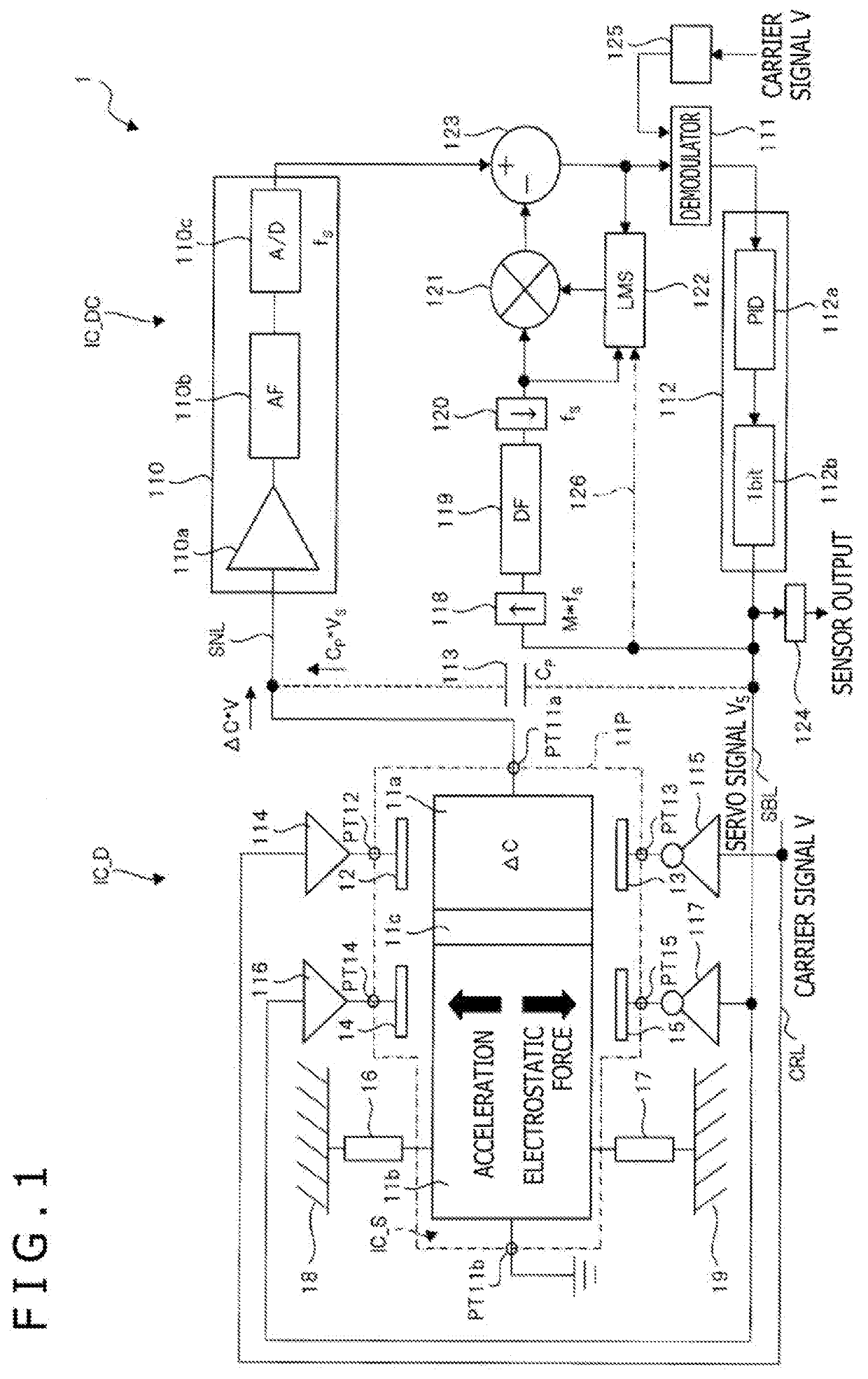
[0028]FIG. 1 is a block diagram illustrating a configuration of an acceleration sensor according to embodiment 1. In FIG. 1, reference numeral 1 denotes an acceleration sensor. In the descriptions given below, an acceleration sensor will be simply referred to as a sensor unless otherwise required to demonstrate that the sensor is an acceleration sensor. The sensor 1 according to embodiment 1 includes, although not limited thereto, three semiconductor devices. For reasons of explanation, the three semiconductor devices included in the sensor 1 will be denoted as a sensor semiconductor device IC_S, a driving semiconductor device IC_D, and a detection / control semiconductor device IC_DC. The sensor semiconductor device IC_S is realized by integrating acceleration sensor elements (hereinafter referred to as sensor elements). The driving semiconductor device IC_D drives the sensor elements on the basis of a servo signal Vs and a carrier signal V. The detection / control semiconductor device...
embodiment 2
[0077]FIG. 2 is a block diagram illustrating a configuration of a sensor according to embodiment 2. FIG. 2 is similar to FIG. 1. Therefore, the difference between the two will be primarily described. The difference from FIG. 1 is that the detection circuit 110 has been changed. In FIG. 2, the detection circuit 110 further includes a tuning circuit 110d. The analog filter 110b is connected to the tuning circuit 110d. The analog filter 110b is set up by the tuning circuit 110d such that the analog filter 110b offers a desired frequency characteristic. The analog filter 110b and the tuning circuit 110d as described above can be realized, for example, by the technology described in non-patent document 2.
[0078]In embodiment 2, the analog filter 110b can be set up by the tuning circuit 110d such that the frequency characteristic of the analog filter 110b in the detection circuit 110 matches the frequency characteristic of the filter realized by the up-sampler 118, the digital filter 119, ...
embodiment 3
[0079]FIG. 3 is a block diagram illustrating a configuration of a sensor according to embodiment 3. FIG. 3 is similar to FIG. 1. Therefore, the difference between the two will be primarily described. FIG. 3 depicts, in detail, the configuration of the C / V conversion amplifier 110a illustrated in FIG. 1.
[0080]The C / V conversion amplifier 110a includes an amplifier 1101a, a capacitive element 1102a, and a resistive element 1103a. The amplifier 1101a includes a so-called op-amp. A given voltage Vb is supplied to a positive phase input node + of the amplifier 1101a, and an inverted input node (−) is connected to the wire SNL. An output node is connected to the input of the analog filter 110b. The capacitive element 1102a and the resistive element 1103a are connected in parallel between the inverted input node (−) and the output terminal of the amplifier 110a. As a result, a so-called negative feedback inversion amplifier is formed. In this configuration, the charge signal (ΔC*V) in the ...
PUM
 Abstract
Description
Claims
Application Information