Method of manufacturing multilayer ceramic electronic component and multilayer ceramic electronic component

Active Publication Date: 2020-04-09
SAMSUNG ELECTRO MECHANICS CO LTD
View PDF0 Cites 4 Cited by
  • Summary
  • Abstract
  • Description
  • Claims
  • Application Information

AI Technical Summary

Benefits of technology

The present invention provides a method for making a multilayer ceramic electronic component that has reliable and high capacitance performance. The technical effect is the ability to make a more efficient and reliable device that meets specific performance requirements.

Problems solved by technology

However, as capacitance is significantly decreased in an environment of 150° C. or more due to unique characteristics of barium titanate (BaTiO3) oxide, it is difficult to secure electrical characteristics depending on a temperature required by electrical components.
In addition, it is impossible to use the multilayer ceramic capacitor in an environment up to 200° C. Therefore, the development of a multilayer ceramic capacitor that may be used even in a high temperature environment by applying a new composition has been required.

Method used


Image

  • Method of manufacturing multilayer ceramic electronic component and multilayer ceramic electronic component
  • Method of manufacturing multilayer ceramic electronic component and multilayer ceramic electronic component
  • Method of manufacturing multilayer ceramic electronic component and multilayer ceramic electronic component

Examples


Embodiment Construction

[0020]Hereinafter, exemplary embodiments of the present disclosure will now be described in detail with reference to the accompanying drawings.

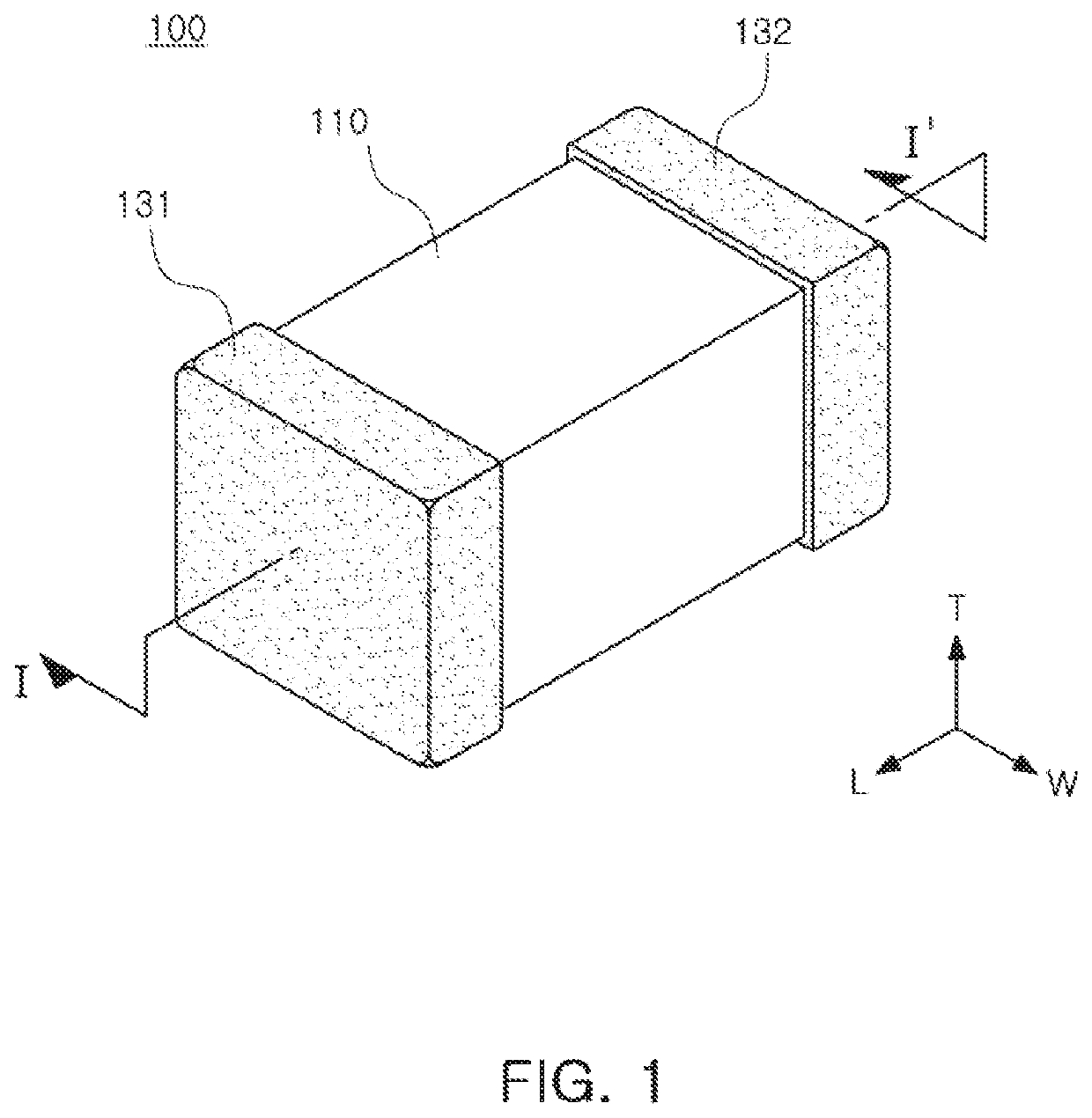
[0021]FIG. 1 is a perspective view illustrating a multilayer ceramic capacitor according to an exemplary embodiment in the present disclosure.

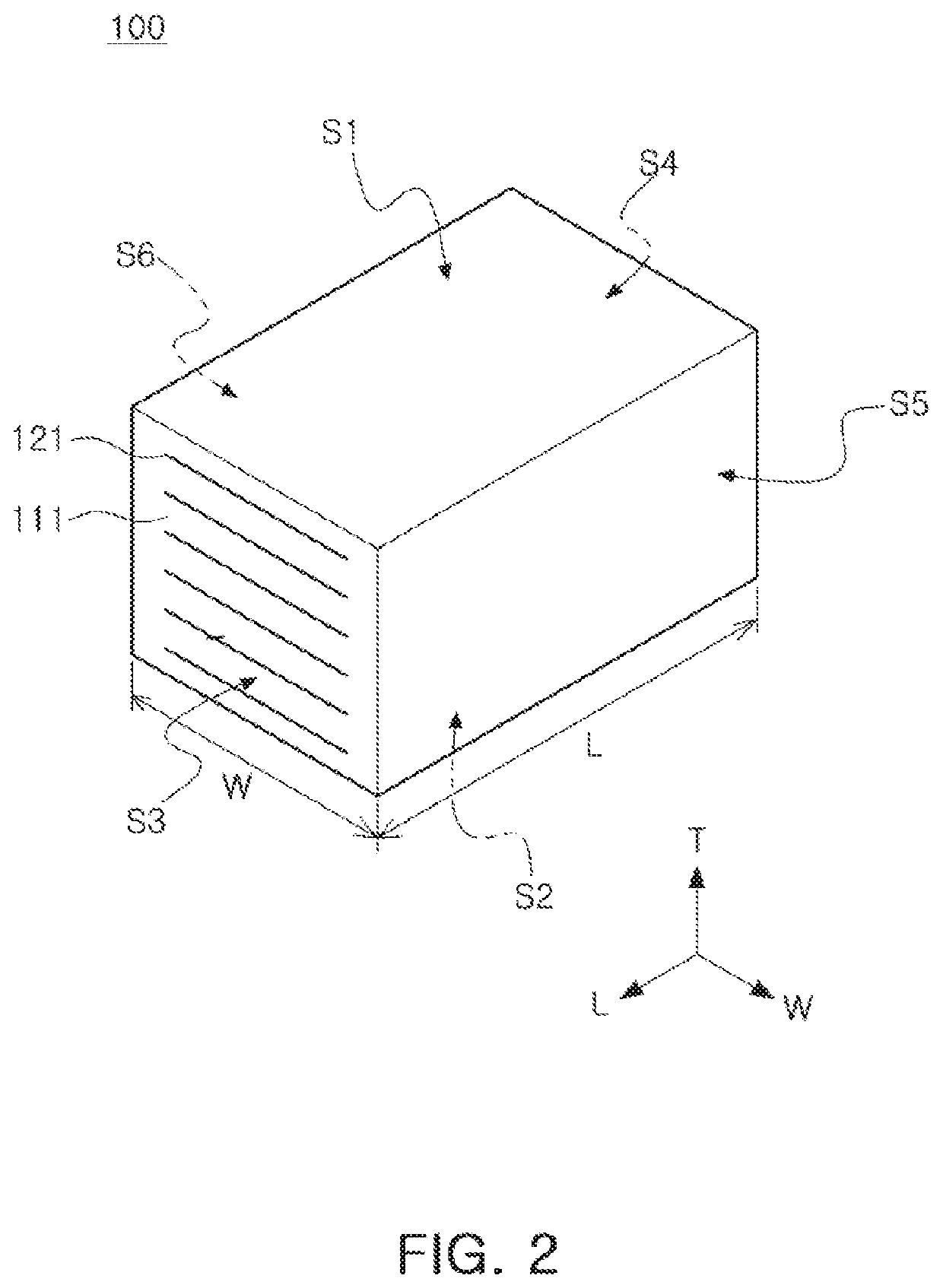
[0022]FIG. 2 is a schematic view illustrating a ceramic body according to an exemplary embodiment in the present disclosure.

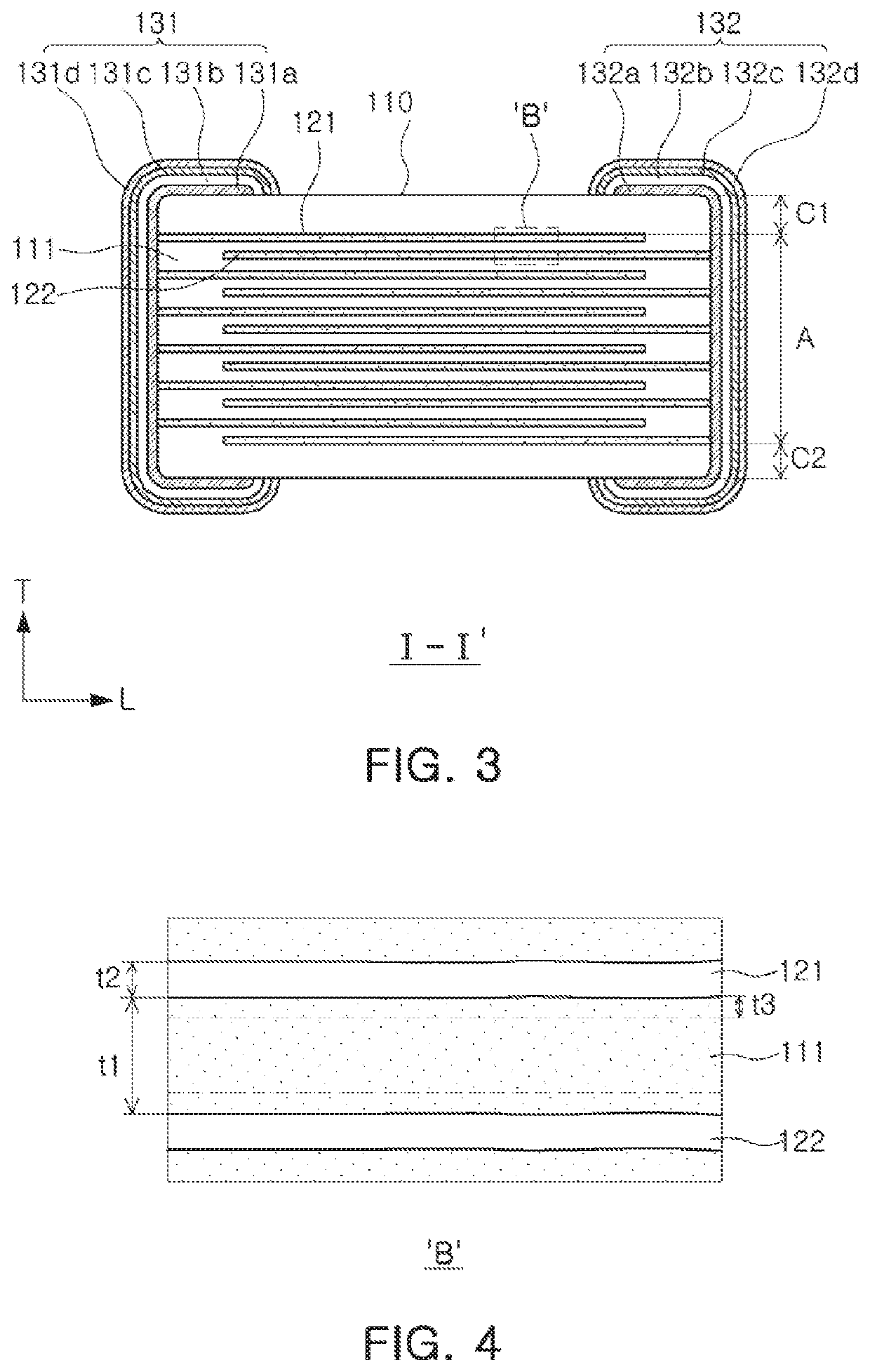
[0023]FIG. 3 is a cross-sectional view taken along line I-I′ of FIG. 1 according to an exemplary embodiment in the present disclosure.

[0024]FIG. 4 is an enlarged view of region B of FIG. 3.

[0025]Referring to FIGS. 1 through 4, a multilayer ceramic electronic component 100 manufactured by a method of manufacturing a multilayer ceramic electronic component according to an exemplary embodiment in the present disclosure may include a ceramic body 110 including dielectric layers 111 and a plurality of first and second internal electrodes 121 and 122 arranged to face each other with each...


PUM

PropertyMeasurementUnit
Thicknessaaaaaaaaaa
Thicknessaaaaaaaaaa
Particle sizeaaaaaaaaaa

Abstract

A method of manufacturing a multilayer ceramic electronic component includes: preparing a dielectric magnetic composition including base material powder particles including BaTi2O5 or (Ba(1-x)Cax)Ti2O5 (0≤x<0.1), the base material powder particles having surfaces coated with one or more of Mg, Mn, V, Ba, Si, Al and a rare earth metal; preparing ceramic green sheets using dielectric slurry including the dielectric magnetic composition; applying an internal electrode paste to the ceramic green sheets; preparing a green sheet laminate by stacking the ceramic green sheets to which the internal electrode paste is applied; and preparing a ceramic body including dielectric layers and a plurality of first and second internal electrodes arranged to face each other with each of the dielectric layers interposed therebetween by sintering the green sheet laminate.

Description

CROSS-REFERENCE TO RELATED APPLICATION(S)[0001]This application claims the benefit of priority to Korean Patent Application No. 10-2018-0118729 filed on Oct. 5, 2018 in the Korean Intellectual Property Office, the disclosure of which is incorporated herein by reference in its entirety.BACKGROUND1. Field[0002]The present disclosure relates to a method of manufacturing a multilayer ceramic electronic component and a multilayer ceramic electronic component, and more particularly, to a method of manufacturing a multilayer ceramic electronic component and a multilayer ceramic electronic component capable of having excellent reliability and a high capacitance.2. Description of Related Art[0003]Recently, in accordance with miniaturization, slimness, and multifunctionalization of electronic products, miniaturization of multilayer ceramic capacitors has also been required, and multilayer ceramic capacitors have also been mounted at a high degree of integration.[0004]A multilayer ceramic capa...

Claims


Application Information

Patent Timeline
IPC IPC(8): H01G4/30H01G4/12H01G4/012C01F11/18
CPCH01G4/30C01F11/188H01G4/1227H01G4/012H01G4/232H01G4/2325C04B35/4686C04B2235/3208C04B35/6281C04B35/62805C04B35/62818C04B35/62807C04B35/62813C04B35/62815B32B18/00C04B2237/346C04B2237/704C04B2235/3236C04B2235/5445C04B35/465C04B2235/3215C04B2235/3418C04B2235/36C04B2235/3203C04B2235/445C04B2235/443C04B2235/3224C04B2235/3227C04B2235/652C04B2235/6582Y02T10/70H01G4/005H01G4/252
Inventor CHOI, DU WONWOO, SEOK KYOONJO, JI HONG
Owner SAMSUNG ELECTRO MECHANICS CO LTD
Why Eureka
Try Eureka