Component Having Enhanced Efficiency and Method for Production Thereof

a technology of components and efficiency, applied in the field of components, can solve problems such as efficiency loss of optoelectronic components, and achieve the effect of increasing efficiency

Active Publication Date: 2020-04-16
OSRAM OLED
View PDF0 Cites 7 Cited by
  • Summary
  • Abstract
  • Description
  • Claims
  • Application Information

AI Technical Summary

Benefits of technology

[0004]Embodiments provide a component having increased efficiency. ...

Problems solved by technology

In optoelectronic components, which are based on a semiconductor material and comprise an active zone, in particular a multiple quantum well structure, it has been ...

Method used


Image

  • Component Having Enhanced Efficiency and Method for Production Thereof
  • Component Having Enhanced Efficiency and Method for Production Thereof

Examples


Embodiment Construction

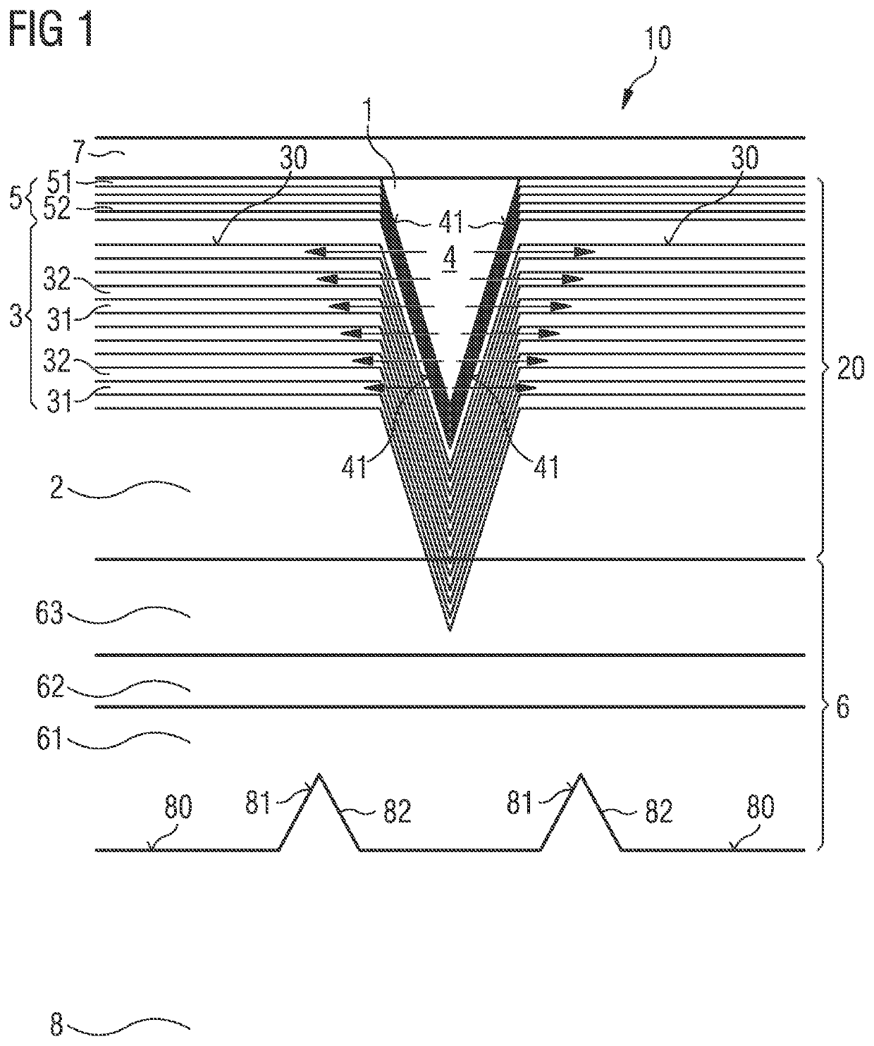
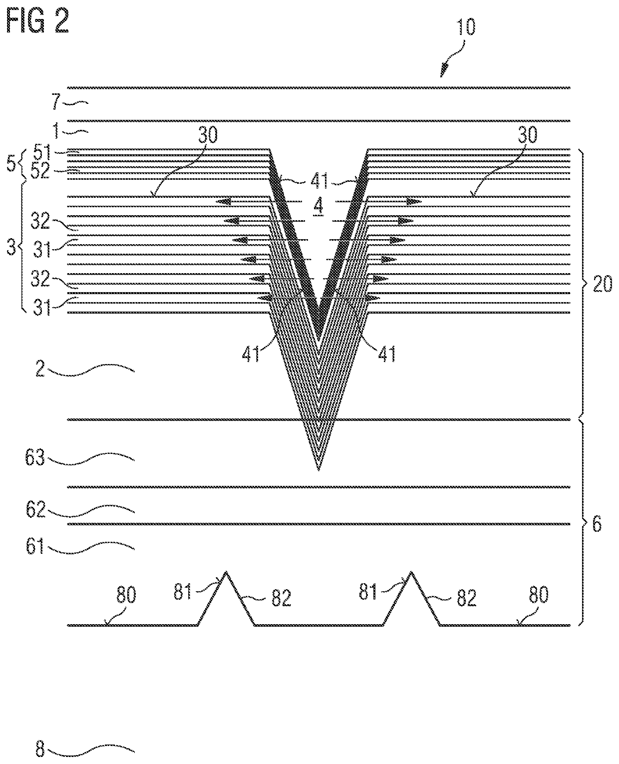
[0036]FIG. 1 shows a component 10 having a carrier 8 on which a semiconductor layer sequence 20 is arranged. The carrier 8 can be a growth substrate on which the semiconductor layer sequence 20 has been epitaxially grown, for example. The semiconductor layer sequence 20 has an active zone 3 which is arranged between a first, for instance p-conducting semiconductor layer 1, and a second, for instance n-conducting semiconductor layer 2. In particular, the active zone 3 is configured for generating electromagnetic radiation during operation of the component 10.

[0037]The active zone 3 has a multiple quantum well structure comprising a plurality of alternating quantum well layers 31 and quantum barrier layers 32. The number of quantum well layers 31 is at least 3 or at least 5 and is, for example, between 3 and 20 inclusive, for instance between 3 and 15 inclusive, for instance 9. The quantum well layers 31 and quantum barrier layers 32 may be based on a III-V compound semiconductor mate...


PUM


Abstract

A component having an enhanced efficiency and a method for producing a component are disclosed. In an embodiment, a component includes a semiconductor layer sequence comprising a p-conducting semiconductor layer, an n-conducting semiconductor layer and an active zone located therebetween, wherein the active zone comprises recesses on a side of the p-conducting semiconductor layer, each recess having facets extending obliquely to a main surface of the active zone, and wherein the p-conducting semiconductor layer extends into the recesses, and a barrier structure, wherein the active zone is arranged between the barrier structure and the n-conducting semiconductor layer so that an injection of positively charged charge carriers into the active zone via the main surface is hindered in a targeted manner so that an injection of positively charged charge carriers into the active zone via the facets is promoted.

Description

[0001]This patent application is a national phase filing under section 371 of PCT / EP2017 / 062000, filed May 18, 2017, which claims the priority of German patent application 10 2016 208 717.7, filed May 20, 2016, each of which is incorporated herein by reference in its entirety.TECHNICAL FIELD[0002]The present application relates to a component having uniform current injection and a method for producing a component.BACKGROUND[0003]In optoelectronic components, which are based on a semiconductor material and comprise an active zone, in particular a multiple quantum well structure, it has been shown that charge carriers within the active zone are not evenly distributed over the entire active zone, resulting in efficiency losses of such optoelectronic components.SUMMARY OF THE INVENTION[0004]Embodiments provide a component having increased efficiency. Embodiments further provide an efficient method for producing a component.[0005]According to at least one embodiment of a component, it ha...

Claims


Application Information

Patent Timeline
IPC IPC(8): H01L33/24H01L33/38H01L33/32H01L33/06H01L33/00H01L33/18
CPCH01L33/325H01L33/007H01L33/38H01L33/18H01L33/24H01L33/06H01L33/025H01L33/04H01L33/14H01L33/145H01L33/32
Inventor LEHNHARDT, THOMASBERGBAUER, WERNEROFF, JÜRGENLAHOURCADE, LISEDRECHSEL, PHILIPP
Owner OSRAM OLED
Why Eureka
Try Eureka