Semiconductor device and method of forming the same

a semiconductor device and semiconductor technology, applied in the direction of semiconductor devices, electrical devices, transistors, etc., can solve the problems of high cost, current lithography technology bottleneck, etc., and achieve the effect of improving the overall component density of the semiconductor device, improving the possibility of current leakage or unstable current issues, and improving isolation

Active Publication Date: 2020-04-23
UNITED MICROELECTRONICS CORP
View PDF7 Cites 6 Cited by
  • Summary
  • Abstract
  • Description
  • Claims
  • Application Information

AI Technical Summary

Benefits of technology

[0004]One object of the present invention is to provide a semiconductor device and a method of forming the same, in which, a dummy cell region is directly disposed on a boundary of a core region to cross the the boundary of the core region, so as to reduce the density difference between each component pattern of the semiconductor device, and also to improve the unstable current issue.
[0007]In summary, the semiconductor device of the present invention disposes at least one dummy cell region on a boundary of a core region, to make the dummy cell region to partially overlap with the core region. In this way, the requested disposing area of the dummy cell region in the semiconductor device is sufficiently shrunk, while maintaining the overall component density of the semiconductor device. Furthermore, the dummy cell region includes an isolation structure which is additionally disposed across the boundary of the core region to overlap with the boundary, with the disposition of the isolation structure improving possible current leakage or unstable current issues occurred at the boundary of the core region. The isolation structure has an extended length on the boundary which is entirely extended over the length of a main element in the core region, so as to achieve a better isolation.

Problems solved by technology

However, as feature sizes are decreased by the complexity of currently integrated circuits to improve the performance of the metal oxide half-field effect transistor, the existing processes have met its bottleneck in currently lithography techniques and the highly cost thereof.

Method used


Image

  • Semiconductor device and method of forming the same
  • Semiconductor device and method of forming the same
  • Semiconductor device and method of forming the same

Examples


first embodiment

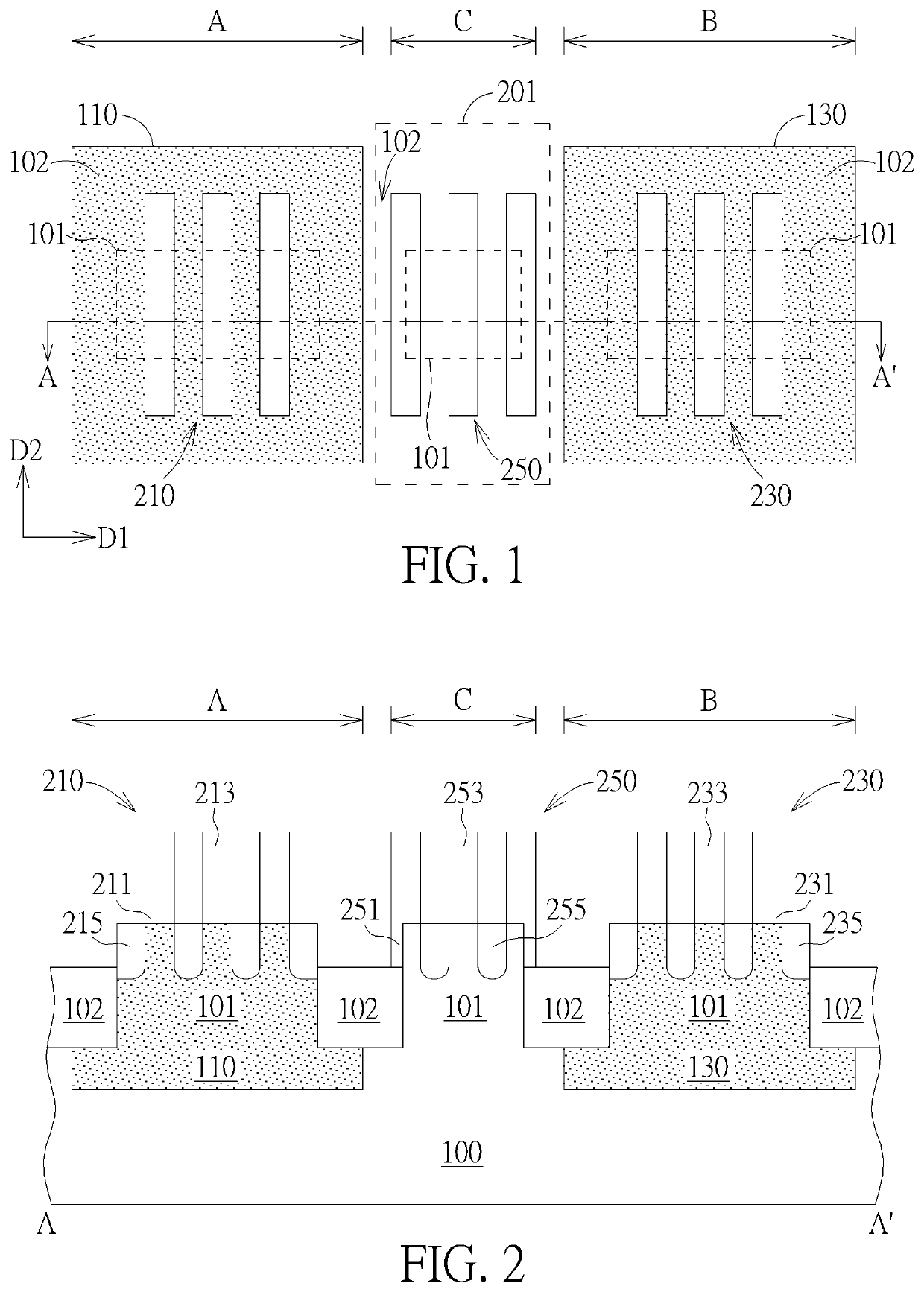
[0024]Please refers to FIGS. 1-2, which are schematic diagrams illustrating a structure of a semiconductor device according to the present invention. First of all, a substrate 100 such as a semiconductor substrate like a silicon substrate, a silicon-containing substrate or a silicon-on-insulator (SOI) substrate is provided, and two wells 110, 130 are further disposed in the substrate 100 to respectively define two regions A, B and a region C between the two regions A, B within the substrate 100. In the present embodiment, the wells 110, 130 preferably include different conductive types such as P-type and N-type, but not limited thereto. In another embodiment, the two wells 110, 130 may optionally include the same conductive type, such as both being P-type or N-type.

[0025]Moreover, at least one fin 101 such as three fins as shown in FIG. 1 are formed in the substrate 100, the fins 101 are paralleled extended in serial, along a direction D1 (such as the x-direction) and a portion of t...

second embodiment

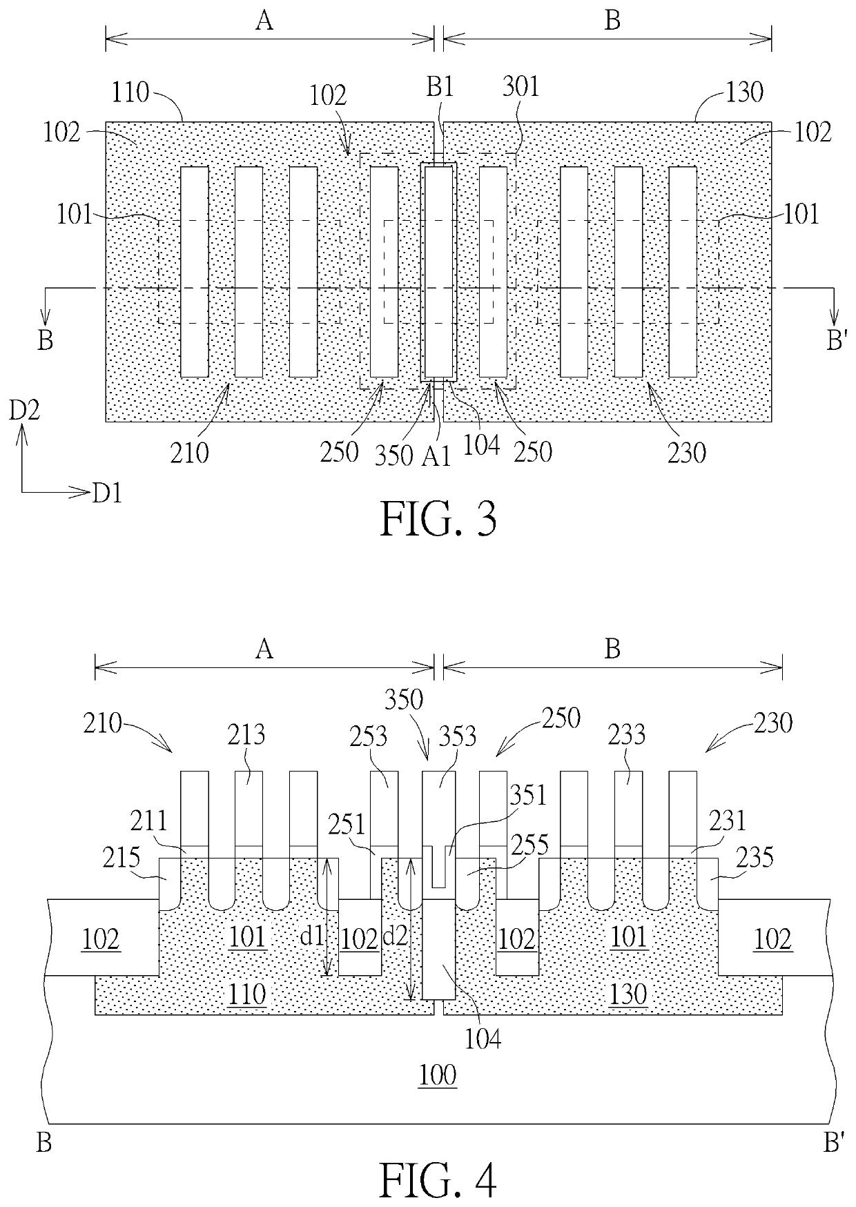
[0030]Please refers to FIGS. 3-4, which are schematic diagrams illustrating a structure of a semiconductor device according to the present invention. The structure in the present embodiment are substantially similar to those in the aforementioned first preferred embodiment, such as including elements like the substrate 100, the fins 101, the shallow trench isolation 102 and the gate structures 210, 230, 250 which will not redundantly described herein after. The differences between the present embodiment and the aforementioned embodiment is mainly in that, a dummy cell region 301 of the present embodiment is partially overlapped with the regions A, B, and the dummy cell region 301 is directly disposed on the boundaries A1, B1 of the regions A, B, across the boundaries A1, B1.

[0031]Precisely speaking, the dummy cell region 301 of the present embodiment includes an isolation structure 104 additionally disposed on the boundaries A1, B1 of the regions A, B, with the isolation structure 1...

third embodiment

[0035]Please refers to FIGS. 8-9, which are schematic diagrams illustrating a structure of a semiconductor device according to the present invention. The structure in the present embodiment are substantially similar to those in the aforementioned second preferred embodiment, such as including elements like the substrate 100, the fins 101, the shallow trench isolation 102 and the gate structures 210, 230, 250 which will not redundantly described herein after. The differences between the present embodiment and the aforementioned embodiment is mainly in that, dummy cell regions 301, 401 of the present embodiment are simultaneously disposed on boundaries A1, A2, B1, B2 of the regions A, B.

[0036]Precisely speaking, in the semiconductor device of the present embodiment, the isolation structures 104, 106 are respectively disposed both on two adjacent boundaries A1, B1 of the regions A, B and on another two boundaries A2, B2 of the regions A, B. The isolation structure 104 is extended along...


PUM

PropertyMeasurementUnit
depthaaaaaaaaaa
densityaaaaaaaaaa
densitiesaaaaaaaaaa

Abstract

A semiconductor device and a method of forming the same, the semiconductor device includes a substrate, a first well and a first dummy cell region. The substrate has a plurality fins disposed therein, and the fins are extended along a first direction. The first well is disposed in the substrate, and a dummy cell region is disposed at a first boundary of the first well. The first dummy cell region includes a first isolation structure and a plurality of first gate structures. The first SDB is disposed in the substrate, along a second direction perpendicular to the first direction to penetrate through one of the fins, and the first gate structures are disposed over the first SDB.

Description

BACKGROUND OF THE INVENTION1. Field of the Invention[0001]The present invention generally relates to the field of a semiconductor device and a method of forming the same, and more particularly to a semiconductor device having a dummy structure and a method of forming the same.2. Description of the Prior Art[0002]In semiconductor processing, dummy patterns have been used in diffusion mask and / or gate layer to prevent dishing effects from chemical-mechanical polishing (CMP) and to minimize the effects of device-to-device variations in pattern density. Accordingly, a shallow trench isolation structure (STI structure) is provided thereby to apply to deep sub-micron process. The formation of the shallow trench isolation structure involves etching of trenches patterns into a semiconductor substrate and subsequently filling the trenches with an insulating material. The insulating material is then planarized by using a process such as a CMP or an etch back process, to form an insulating reg...

Claims


Application Information

Patent Timeline
Patent Type & Authority Applications(United States)
IPC IPC(8): H01L27/088H01L29/06H01L29/78H01L29/66H01L21/8234
CPCH01L21/823431H01L21/823481H01L29/66606H01L21/823437H01L29/7851H01L29/0642H01L29/0696H01L27/0886H01L27/088
Inventor WANG, MENG-CHIANGSHENG, YI-CHUNGHSUEH, SHENG-YUANLEE, KUO-HSING
Owner UNITED MICROELECTRONICS CORP
Why Eureka
Try Eureka