

Pixel array substrate
a technology of pixel array and substrate, applied in the direction of basic electric elements, electrical apparatus, semiconductor devices, etc., can solve the problems of flicker and crosstalk, pixel array may exhibit problems, and the display frame may exhibit problems, and achieve the effect of ultra-high resolution and favorable electrical properties
- Summary
- Abstract
- Description
- Claims
- Application Information
AI Technical Summary
Benefits of technology
Problems solved by technology
Method used
Image

Examples
first embodiment
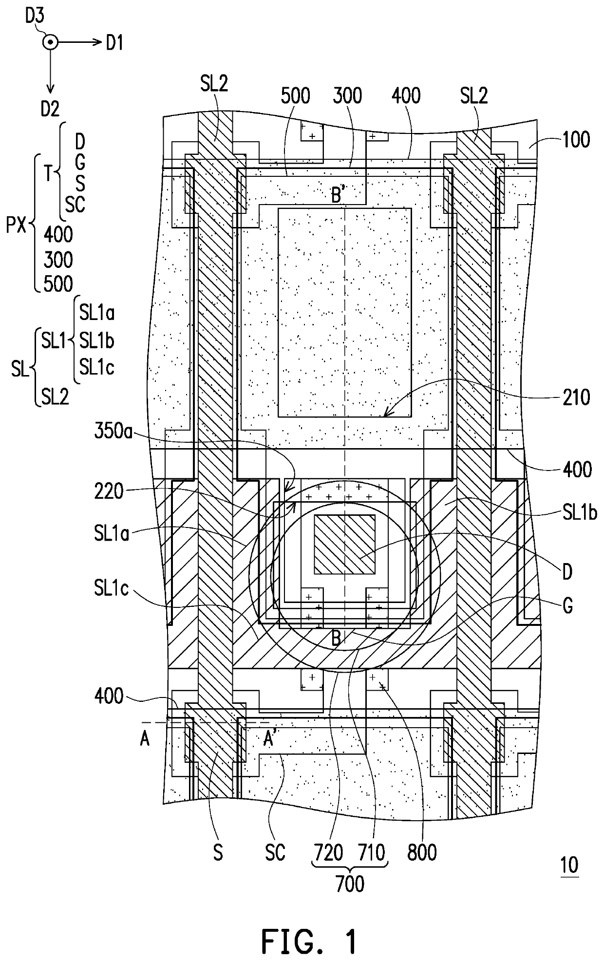
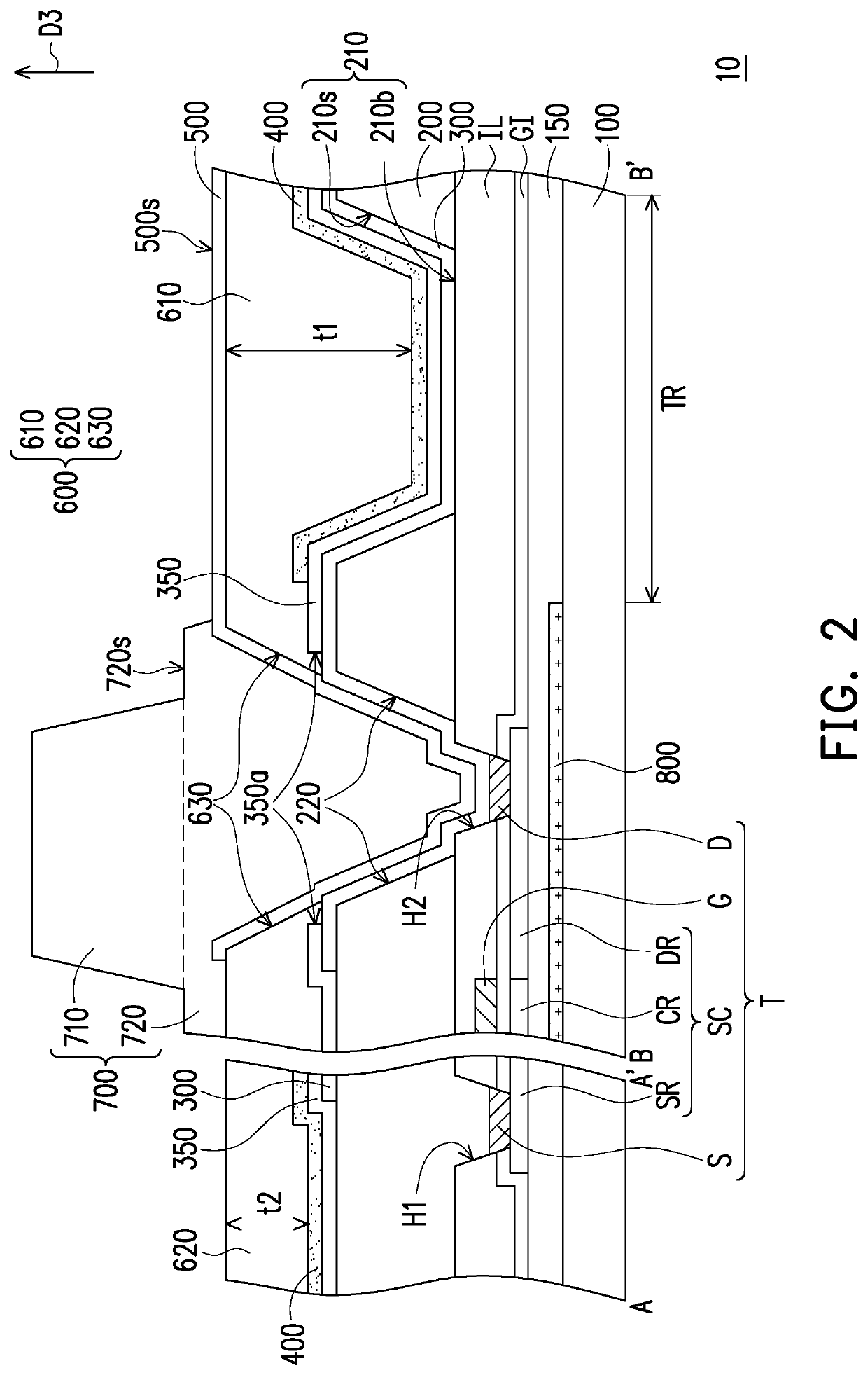
[0041]FIG. 1 is a schematic top view illustrating a pixel array substrate 10 according to the invention. FIG. 2 is a schematic cross-sectional view illustrating the pixel array substrate 10 of FIG. 1. FIG. 2 corresponds to a sectional line A-A′ and a sectional line B-B′ of FIG. 1. It should be noted that, for the ease of illustration, an insulation layer 150, a gate insulation layer GI, an interlayer insulation layer IL, a planarization layer 200, a first insulation layer 350, and a color filter layer 600 shown in FIG. 2 are omitted in FIG. 1.
[0042]Referring to FIG. 1, the pixel array substrate 10 includes a substrate 100, a plurality of pixel structures PX, and a plurality of signal lines SL. The pixel structures PX are arranged into an array on the substrate 100. In the embodiment, the signal lines SL includes a first signal line SL1 and second signal lines SL2 in FIG. 1. The first signal line SL1 and the second signal line SL2 are disposed to intersect each other on the substrate...
second embodiment
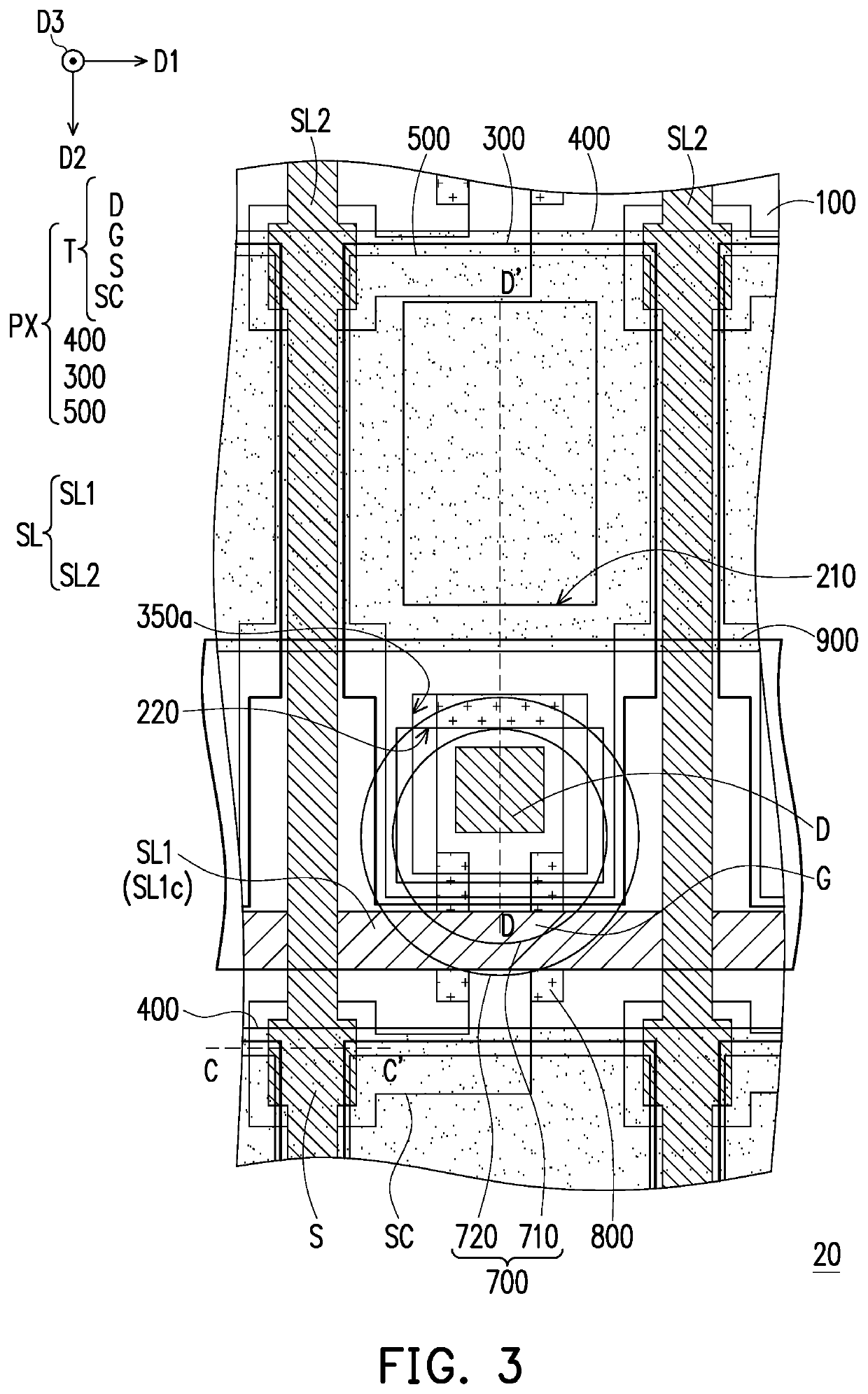
[0063]FIG. 3 is a schematic top view illustrating a pixel array substrate 20 according to the invention. FIG. 4 is a schematic cross-sectional view illustrating the pixel array substrate 20 of FIG. 3. FIG. 4 corresponds to a sectional line C-C′ and a sectional line D-D′ of FIG. 3. It should be noted that, for the ease of illustration, the insulation layer 150, the gate insulation layer GI, the interlayer insulation layer IL, the planarization layer 200, the first insulation layer 350, and the color filter layer 600 shown in FIG. 4 are omitted in FIG. 3.
[0064]Referring to FIG. 3 and FIG. 4, the pixel array substrate 20 of the embodiment differs from the pixel array substrate 10 shown in FIG. 1 and FIG. 2 in that the first signal line SL1 of the pixel array substrate 20 only includes the extending part SL1c, and the pixel array substrate 20 further includes a metal layer 900 disposed between the third conductive layer 500 and the spacer 700 and overlapped with the second opening 220 o...
third embodiment
[0066]FIG. 5 is a schematic top view illustrating a pixel array substrate 30 according to the invention. FIG. 6 is a schematic cross-sectional view illustrating the pixel array substrate 30 of FIG. 5. FIG. 6 corresponds to a sectional line E-E′ and a sectional line F-F′ of FIG. 5. It should be noted that, for the ease of illustration, the insulation layer 150, the gate insulation layer GI, the interlayer insulation layer IL, the planarization layer 200, the first insulation layer 350, and the color filter layer 600 shown in FIG. 6 are omitted in FIG. 5.
[0067]Referring to FIG. 5 and FIG. 6, the pixel array substrate 30 of the embodiment differs from the pixel array substrate 10 shown in FIG. 1 and FIG. 2 in that the first signal line SL1 of the pixel array substrate 30 only includes the extending part SL1c, and a base part 720A of a spacer 700A of the pixel array substrate 30 fills the third opening 630 of the color filter layer 600 and the second opening 220 of the planarization lay...
PUM
| Property | Measurement | Unit |
|---|---|---|
| reflectivity | aaaaa | aaaaa |
| thickness | aaaaa | aaaaa |
| thickness | aaaaa | aaaaa |
Abstract
Description
Claims
Application Information