Organic el display apparatus and manufacturing method therefor

a technology of organic el and display apparatus, which is applied in the direction of identification means, semiconductor/solid-state device details, instruments, etc., can solve the problems of uneven surface of the surface, and achieve the suppression of luminance unevenness, low resistance, and high luminance.

Active Publication Date: 2020-05-28
SAKAI DISPLAY PROD
View PDF0 Cites 12 Cited by
  • Summary
  • Abstract
  • Description
  • Claims
  • Application Information

AI Technical Summary

Benefits of technology

[0025]According to embodiments of the present invention, it is ensured that the electrical connection be made between the drive circuit and the organic light emitting element regardless of the pixel, and also the electrical connection is made at a low resistance, so that each pixel emits light uniformly at a high luminance. Moreover, the surface of the planarizing layer is planarized to form the first electrode of the organic light emitting element on the surface thereof by sputtering or the like, so that the surface of the organic light emitting layer is also planar and there is no inclined surface due to unevenness of the light emitting surface even when viewed microscopically, so that light at the center of light emission is emitted toward the display screen. Therefore, luminance unevenness and / or chromaticity unevenness is suppressed, making it possible to substantially increase the display definition of the organic EL display apparatus.

Problems solved by technology

When the drive circuit including TFT is formed, the surface thereof becomes uneven.

Method used


Image

  • Organic el display apparatus and manufacturing method therefor
  • Organic el display apparatus and manufacturing method therefor
  • Organic el display apparatus and manufacturing method therefor

Examples


example 1

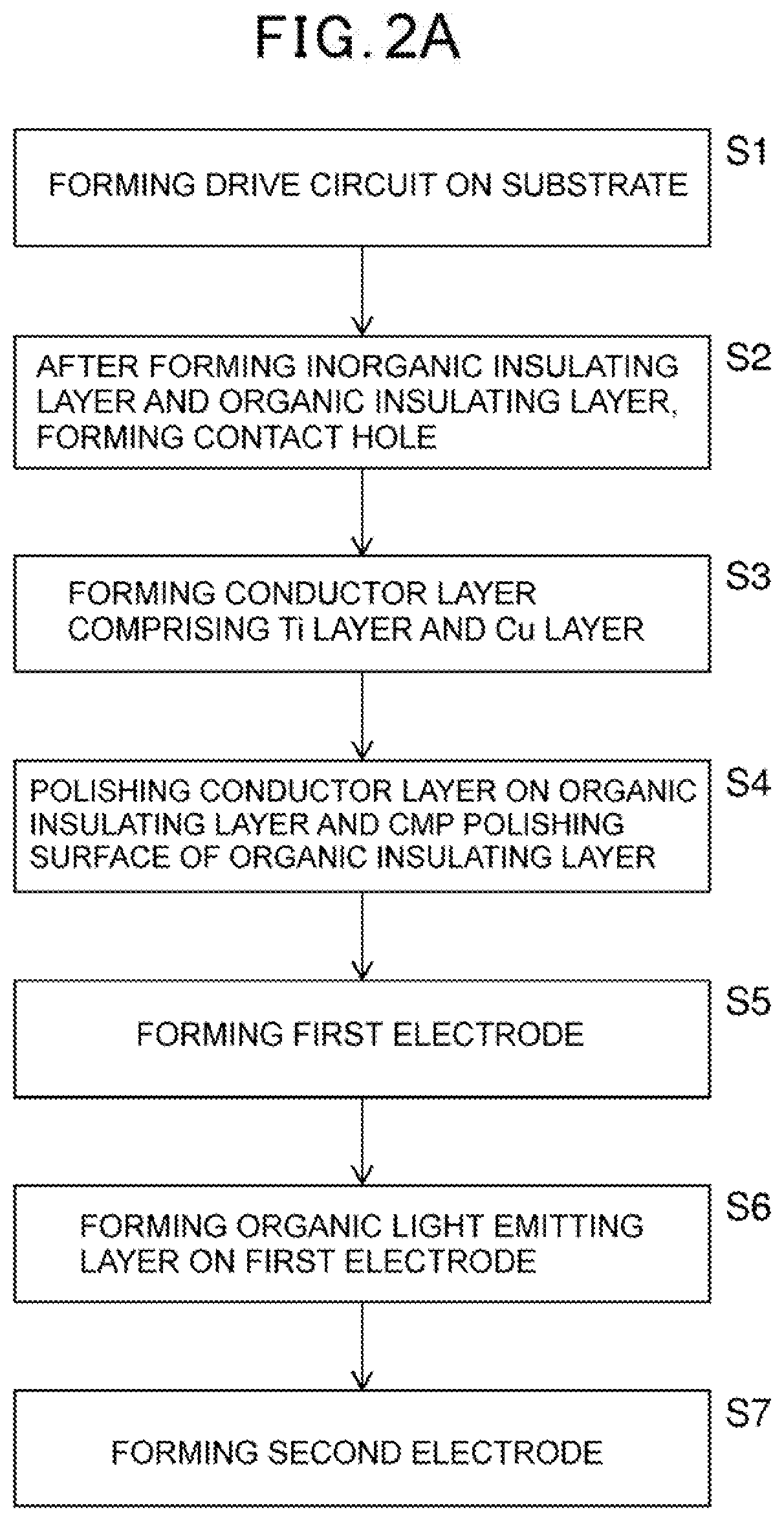
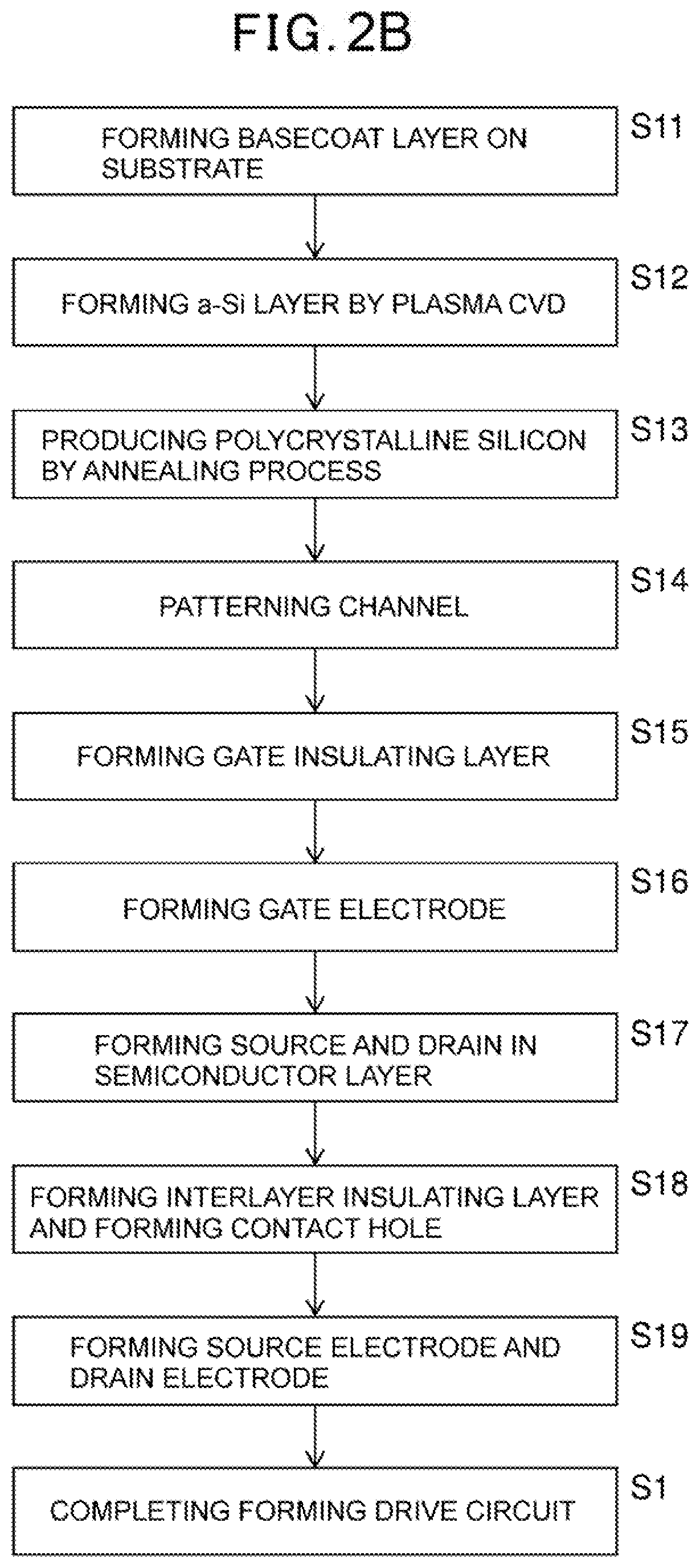
[0062]A method of manufacturing the organic EL display apparatus shown in FIG. 1 is described with reference to flowcharts in FIGS. 2A to 2B and manufacturing processes in FIGS. 3A to 3G below.

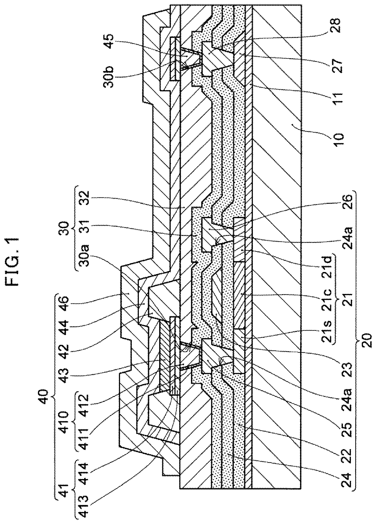
[0063]First, as shown in FIG. 3A, a drive circuit comprising a TFT 20 is formed on a substrate 10 (S1 in FIG. 2A). More specifically, as shown with the flowchart in FIG. 2B, a basecoat layer 11 is formed on the substrate 10 (S11). The basecoat layer 11 is formed by, using plasma CVD, for example, an SiO2 layer with the thickness of approximately 500 nm, and forming thereon an SiNx layer with the thickness of approximately 50 nm to deposit the lower layers, and further depositing the SiO2 layer with the thickness of 250 nm as an upper layer thereof.

[0064]Thereafter, on the basecoat layer 11 is formed a semiconductor layer 21 comprising an amorphous silicon (a-Si) layer by reduced pressure plasma CVD, for example. (S12). Thereafter, an annealing process is conducted for approximately 45 minutes ...

example 2

[0081]In the method of manufacturing according to Example 1 as shown in FIGS. 2A to 2B and FIGS. 3A to 3G, with the planarizing layer 30, the inorganic insulating layer 31 and the organic insulating layer 32 are continuously formed and the contact holes 30a are formed in a collective manner. However, it can be made such that the organic insulating layer 32 being photosensitive is formed as the organic insulating layer 32, the first contact hole 30al is formed after the inorganic insulating layer 31 is formed, after which the organic insulating layer 32 being photosensitive is formed, the second contact hole 30a2 is formed by exposure and development, resulting in contact holes 30a, an example of which is shown FIGS. 4A and 4B.

[0082]More specifically, the previously described processes shown in FIG. 3A are performed in the same manner as in Example 1. Thereafter, as shown in FIG. 4A, after the inorganic insulating layer 31 is formed, the first contact hole 30al is formed at a locatio...


PUM

PropertyMeasurementUnit
surface roughnessaaaaaaaaaa
arithmetic average roughness Raaaaaaaaaaa

Abstract

The present invention is equipped with: a substrate (10) that has a surface upon which a drive circuit containing a TFT (20) is formed; a planarization film (30) that makes the surface of the substrate planar by covering the drive circuit; and an organic light-emitting element (40) that is provided with a first electrode (41) formed upon the surface of the planarization film and connected to the drive circuit, an organic light-emitting layer (43) formed upon the first to electrode, and a second electrode (44) formed upon the organic light-emitting layer. In addition, the planarization film has a two-layer structure comprising an inorganic insulating film (31) and an organic insulating film (32) that are layered upon the TFT, a conductor layer containing a titanium layer and a copper layer is embedded in the interior of a contact hole, and the first electrode is formed electrically connected to the conductor layer.

Description

TECHNICAL FIELD[0001]The present invention relates to an organic EL display apparatus and a manufacturing method thereof.BACKGROUND ART[0002]In recent years, there has been a tendency for organic EL display apparatuses to be adopted in large-sized televisions and mobile devices. An organic EL display apparatus is configured with a drive circuit being formed in a region of each pixel, the drive circuit using a thin film transistor (also called TFT below) as active elements such as a switching element and a drive element, and an organic light emitting element of each pixel being formed thereon so as to be connected to the TFT. The types of organic EL display apparatuses comprise a top emission type with the top surface of a light emitting element as a display surface and a bottom emission type with the rear surface of an insulating substrate as a display surface. With the top emission type, regardless of a display region of the organic light emitting element, the previously described ...

Claims


Application Information

Patent Timeline
Patent Type & Authority Applications(United States)
IPC IPC(8): H01L27/32H01L51/56H05B44/00
CPCH01L51/56H01L27/3276H01L2227/323H01L27/3258G09F9/00G09F9/30H01L21/3205H01L21/321H01L21/768H01L23/532H05B33/10H05B33/22H05B33/26H01L27/1248H01L27/124Y02B20/30H05B44/00H10K59/00H10K59/123H10K59/124H10K50/00H10K59/131H10K71/00H10K59/1201
Inventor KISHIMOTO, KATSUHIKO
Owner SAKAI DISPLAY PROD
Why Eureka
Try Eureka