
Photoelectric conversion device, method of manufacturing photoelectric conversion device, and method of manufacturing semiconductor device

a technology of photoelectric conversion device and conversion circuit, which is applied in the direction of semiconductor/solid-state device testing/measurement, television system, radio frequency controlled devices, etc., can solve the problem that the photoelectric conversion device having the inspection circuit cannot obtain compatibility between a higher degree of integration and low noise, voltage fluctuations, and reducing the degree of integration of a semiconductor chip. achieve the effect of low noise and high degree of integration

Active Publication Date: 2020-06-18
CANON KK
View PDF0 Cites 0 Cited by
  • Summary
  • Abstract
  • Description
  • Claims
  • Application Information

AI Technical Summary

Benefits of technology

The patent text describes a new method for connecting an inspection circuit to an external connection pad in a photoelectric conversion device. This method improves the stability of the input or output potential of the inspection circuit, which leads to higher integration and lower noise in the device. The technical effect is to provide a photoelectric conversion device with a high degree of integration and low noise.

Problems solved by technology

The inventors found that if an inspection circuit has an unstable input or output potential, the operation of the inspection circuit may change to an unstable state and cause voltage fluctuations.
In WO 2015 / 159766, however, the external connection pad for stabilizing the input or output potential of the inspection circuit, thereby reducing the degree of integration of a semiconductor chip.
Furthermore, WO 2015 / 159766 does not describe a method (steps) of stabilizing the potential of an inspection circuit unconnected to the external connection pad.
In other words, a photoelectric conversion device having the inspection circuit cannot obtain compatibility between a higher degree of integration and lower noise.

Method used


Image

  • Photoelectric conversion device, method of manufacturing photoelectric conversion device, and method of manufacturing semiconductor device
  • Photoelectric conversion device, method of manufacturing photoelectric conversion device, and method of manufacturing semiconductor device
  • Photoelectric conversion device, method of manufacturing photoelectric conversion device, and method of manufacturing semiconductor device

Examples


embodiment 1

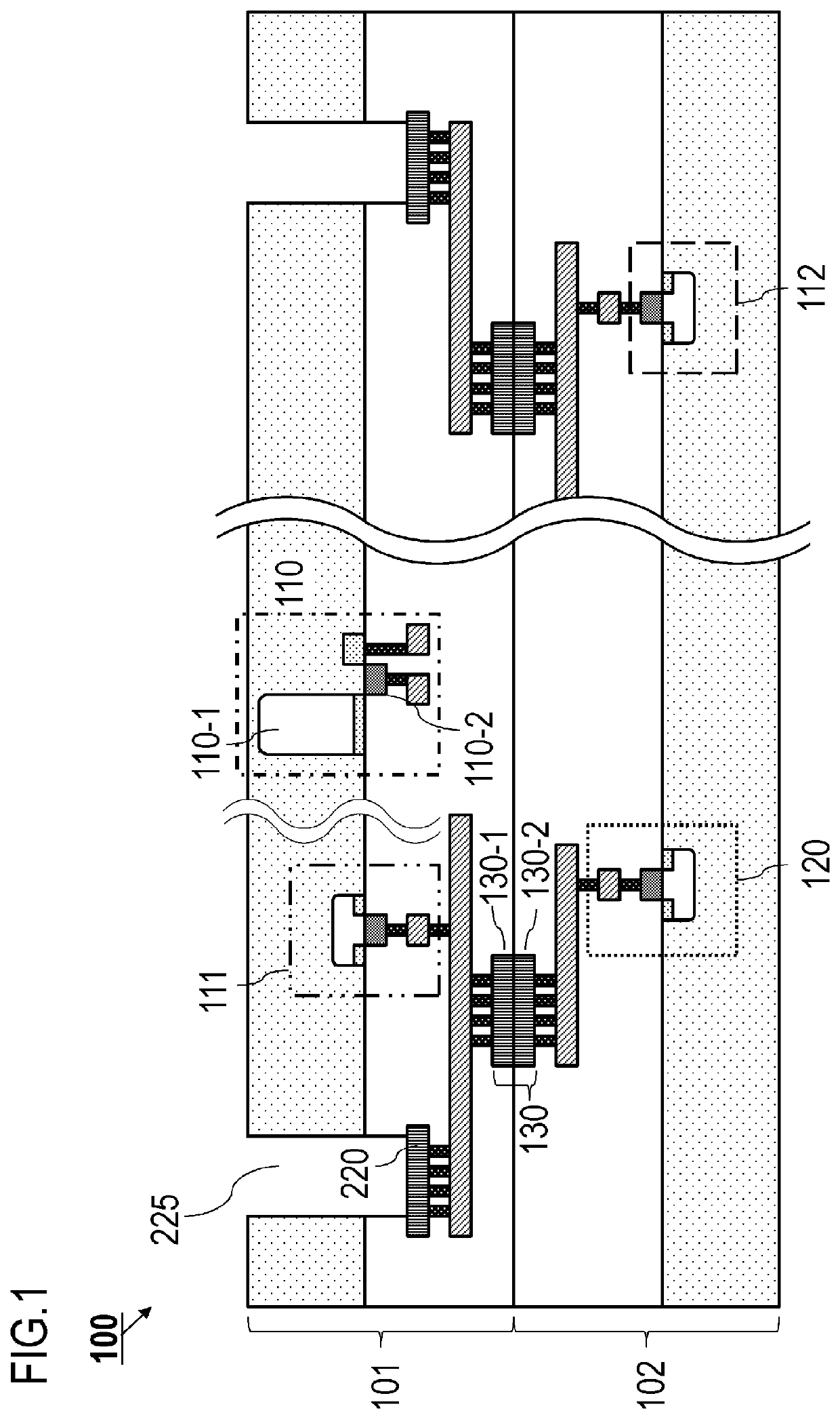
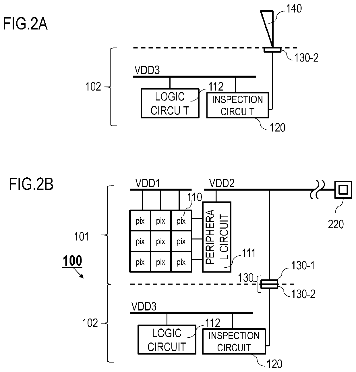
[0067]In Embodiment 1 of the present invention, two semiconductor substrates are stacked in a photoelectric conversion device. A potential (power supply potential) is supplied to an inspection circuit formed on an inspection substrate that is one of the semiconductor substrates and the inspection circuit is connected to another potential on the other semiconductor substrate via a stacked connection part. With this configuration, even if the supplied potential changes, a potential (voltage) on the inspection circuit can be stabilized, thereby suppressing the occurrence of noise. In the present embodiment, an external connection pad is not used for connection to another potential and thus the degree of integration of the photoelectric conversion device improves.

[0068]Referring to FIGS. 1, 2A, and 2B, a solid-state imaging device 100 acting as a photoelectric conversion device (stacked sensor; semiconductor device) according to the present embodiment will be described below.

[0069]Cross...

embodiment 2

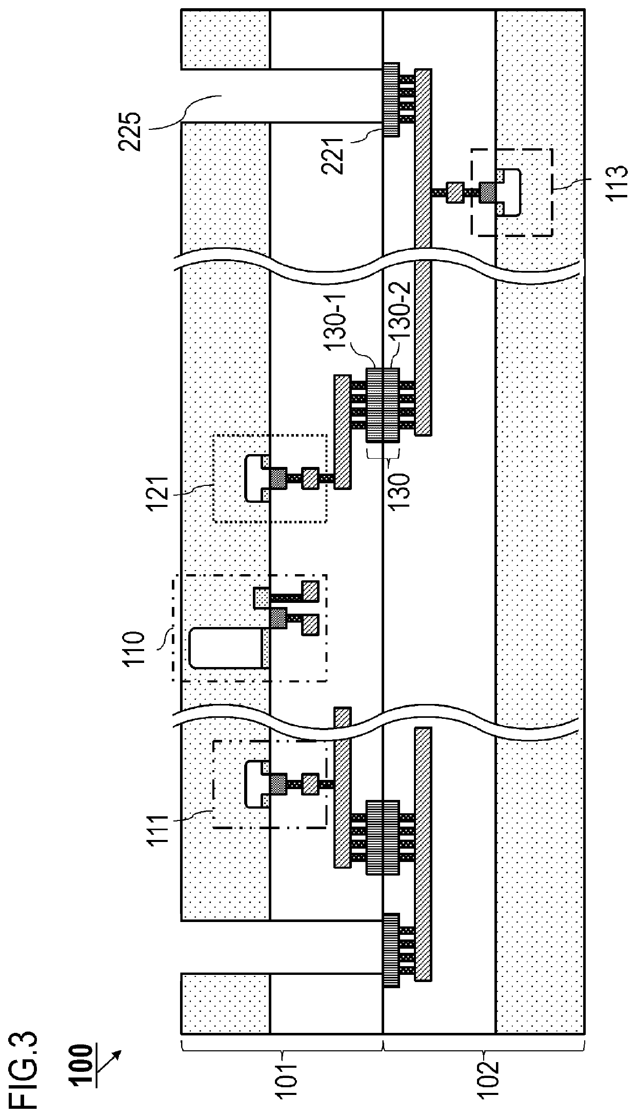
[0085]In the solid-state imaging device according to Embodiment 1, the inspection circuit is formed on the same semiconductor substrate as the logic circuit, whereas in a solid-state imaging device (optical-electrical converter) according to the present embodiment has an inspection circuit on the same semiconductor substrate as a pixel circuit and a peripheral circuit. Referring to FIGS. 3, 4A, 4B, and 5, a solid-state imaging device 100 according to Embodiment 2 will be described below. The same configurations as those of Embodiment 1 are indicated by the same reference numerals and a detailed explanation thereof is omitted.

[0086]Cross-Sectional Configuration of Solid-State Imaging Device

[0087]FIG. 3 is a cross-sectional view of the solid-state imaging device 100. As in Embodiment 1, a semiconductor substrate 101 has a pixel circuit 110 and a peripheral circuit 111 and a semiconductor substrate 102 has a logic circuit 121 (not illustrated). In the present embodiment, the semiconduc...

embodiment 3

[0105]In the solid-state imaging device according to Embodiment 2, one inspection circuit is formed for each one semiconductor substrate, whereas in a solid-state imaging device according to the present embodiment has two inspection circuits on a semiconductor substrate.

[0106]In this case, as in Embodiments 1 and 2, hot carrier luminescence may occur and a false signal may be superimposed on the output signal of the solid-state imaging device if the inputs or outputs of the two inspection circuits have unstable potentials during an operation (driving) of the solid-state imaging device. Additionally, if the two inspection circuits are disposed on the same substrate as a pixel circuit, AC voltage fluctuations of the two inspection circuits may cause the superimposition of a false signal on the output signal of the solid-state imaging device via capacitive coupling.

[0107]If the configurations of Embodiments 1 and 2 are applied in the provision of multiple inspection circuits, it is nec...


PUM


Abstract

A photoelectric conversion device comprising: a first substrate that includes a pixel circuit including a photoelectric conversion element; a second substrate having a signal processing circuit that drives the pixel circuit or processes a signal from the pixel circuit; a connection part electrically connecting the first substrate and the second substrate; and an inspection circuit, wherein the inspection circuit is formed in one of the first and second substrates and is connected to a wire supplying a first potential and being provided in the one of the first and second substrates, and the inspection circuit is connected via the connection part to a wire supplying a second potential and being provided in the other of the first and second substrates.

Description

BACKGROUND OF THE INVENTIONField of the Invention[0001]The present technique relates to a photoelectric conversion device, a method of manufacturing the photoelectric conversion device, and a method of manufacturing a semiconductor device.Description of the Related Art[0002]For CCD or amplifying solid-stage imaging devices used for digital still cameras and camcorders, stacked structures are proposed such that semiconductor chips having different functions are joined to be electrically connected. A solid-state imaging device having such a stacked structure (hereinafter, will be referred to as a photoelectric conversion device) allows formation of an optimum process and an optimum circuit for each semiconductor chip, thereby providing greater functionality with ease. In another proposal, a measurement is performed by an inspection circuit in a photoelectric conversion device before semiconductor chips are joined and then a wafer is selected or rejected or redundant repair is processe...

Claims


Application Information

Patent Timeline
IPC IPC(8): H04N17/00H01L21/66H01L27/146H04N5/372
CPCH01L27/14636H04N17/002H01L27/1469H01L22/34H04N5/379H01L22/14H04N5/372H01L27/14634H04N25/79H04N25/69H04N25/71
Inventor ISHII, RYUNOSUKEOSETO, AKIRAKATO, TATSUNORIWATANABE, TAKANORIKAKINUMA, NOBUAKIKOBAYASHI, HIROAKISAKURAI, KATSUHITO
Owner CANON KK
Learn More