

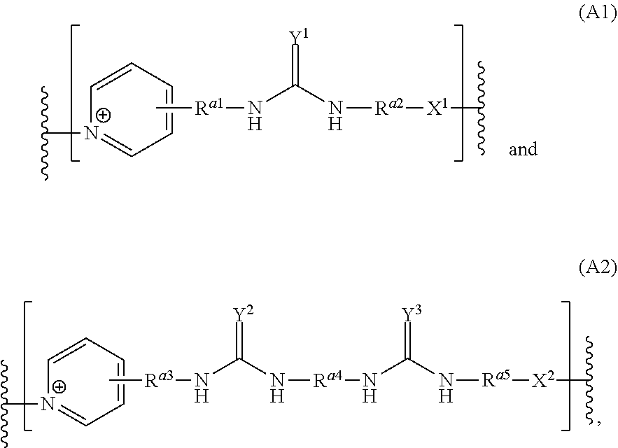
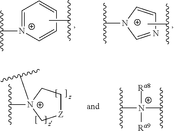
Pyridinium compounds, a synthesis method therefor, metal or metal alloy plating baths containing said pyridinium compounds and a method for use of said metal or metal alloy plating baths
a technology of pyridinium compounds and pyridinium compounds, which is applied in the direction of organic chemistry, semiconductor devices, basic electric elements, etc., can solve the problems that the additives used in acidic copper plating baths are not suitable to meet the current and future requirements in the manufacture of advanced printed circuit boards
- Summary
- Abstract
- Description
- Claims
- Application Information
AI Technical Summary
Benefits of technology
Problems solved by technology
Method used
Image

Examples
application example 1
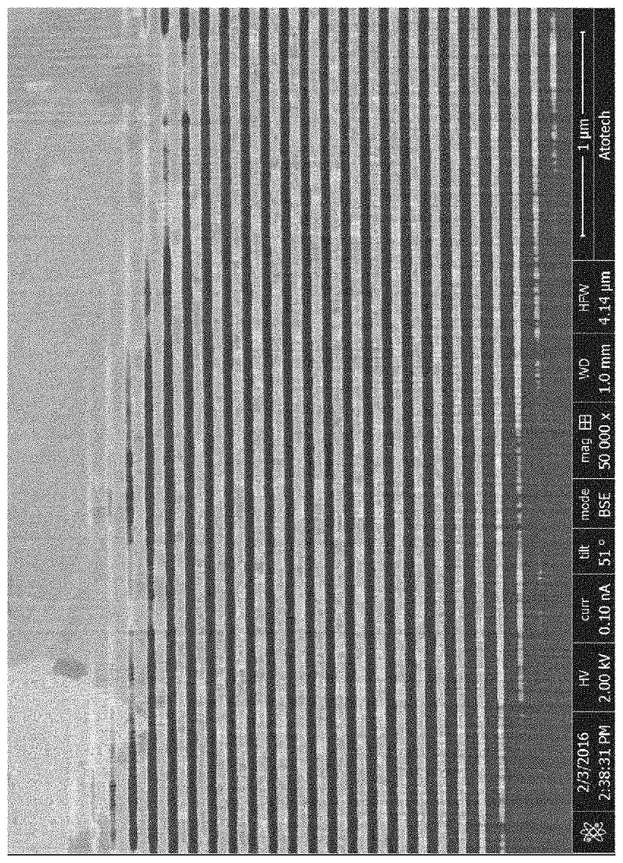
Uniformity (Mounding Properties)
[0132]A solution comprising 5 g / L Cu2+ ions (added as copper sulfate), 10 g / L sulfuric acid, 50 mg / L chloride ions (added as hydrochloric acid), 4 mL / L Atomplate® suppressor and 4.3 mL / L Atomplate® accelerator (both products of Atotech Deutschland GmbH) was used. The pyridinium compounds were added as leveler to said solution in concentration as given in the subsequent table to give the individual copper plating baths.
[0133]Substrates consisting of coupons of approximately 20 mm×25 mm cleaved from a 300 mm 32 nm node test pattern wafer using low-k dielectric. ALL features were 200 nm deep. Features used for these experiments had a line to space ratio of 1:1 and had a pitch of 100 nm. The barrier / Liner / seed stack consisted of 3 nm TaN / 3 nm Ta / 30 nm Cu using industry standard PVD methods on an AMAT Endura tool. The coupons were plating in a beaker-scale coupon plating apparatus where the temperature was 25° C., and the anode was soluble copper separated...
application example 2
[0136]A solution comprising 5 g / L Cu2+ ions (added as copper sulfate), 10 g / L sulfuric acid, 50 mg / L chloride ions (added as hydrochloric acid), 4 mL / L Atomplate® suppressor, 4.3 mL / L Atomplate® accelerator (both products of Atotech Deutschland GmbH) and 3.5 mL / L of pyridinium compound PC1 was used.
[0137]A substrate consisting of coupons of approximately 20 mm×25 mm cleaved from a 300 mm 32 nm node test pattern wafer using low-k dielectric was used. ALL features were 200 nm deep. Features used for these experiments had a line to space ratio of 1:1 and had a pitch of 48 nm. The barrier / Liner / seed stack consisted of 3 nm TaN / 3 nm Ta / 30 nm Cu using industry standard PVD methods on an AMAT Endura tool. The coupons were plating in a beaker-scale coupon plating apparatus where the temperature was 25° C., and the anode was soluble copper separated by a nafion membrane from cathode chamber. The waveform consisted of an entry step followed by three distinct plating steps. The entry step used...
application example 3
osits (SP2 and SP3 Defects)
[0139]As substrates, 300 mm unpatterned wafers with uniform layers as follows were used. The dielectric layer was 100 nm SiO2 formed from tetraethoxysilane. The barrier / liner / seed stack consisted of 4 nm TaN / 2 nm Ta / 45 nm Cu using industry standard PVD methods on an AMAT Endura tool. The wafers were plated in a Sabre® Extreme™ plating tool (LAM Research). The substrates were contacted in said plating tool with a copper plating baths each comprising 5 g / L Cu2+ ions (added as copper sulfate), 10 g / L sulfuric acid, 50 mg / L chloride ions (added as sodium chloride), 4 mL / L Atomplate® suppressor, 4 mL / L Atomplate® accelerator (both products of Atotech Deutschland GmbH) and pyridinium compound PC1 in concentrations as given in the subsequent table where the temperature was 25° C. The waveform consisted of an entry step followed by three distinct plating steps. The entry step used a potential controlled hot entry to match a nominal 16 mA / cm2 at 90 RPM for 0.1 s. T...
PUM
| Property | Measurement | Unit |
|---|---|---|
| concentration | aaaaa | aaaaa |
| weight average molecular mass Mw | aaaaa | aaaaa |
| electrical current | aaaaa | aaaaa |
Abstract
Description
Claims
Application Information