Semiconductor package and manufacturing method thereof

a technology of semiconductor and packaging, applied in the direction of semiconductor/solid-state device details, semiconductor devices, electrical apparatus, etc., can solve the problem of miniaturization of semiconductor packages, and achieve the effect of improving electrical performance and increasing manufacturability

Active Publication Date: 2020-08-27
POWERTECH TECHNOLOGY
View PDF0 Cites 4 Cited by
  • Summary
  • Abstract
  • Description
  • Claims
  • Application Information

AI Technical Summary

Benefits of technology

[0004]The disclosure provides a semiconductor package and a manufacturing method thereof, which provides improvement in electrical performance and greater manufacturability.

Problems solved by technology

Since the chip package technique is highly influenced by the development of integrated circuits, therefore, as the size of electronics has become demanding, so does the package technique.
As such, miniaturizing the semiconductor package while maintaining the process simplicity has become a challenge to researchers in the field.

Method used


Image

  • Semiconductor package and manufacturing method thereof
  • Semiconductor package and manufacturing method thereof
  • Semiconductor package and manufacturing method thereof

Examples


Embodiment Construction

[0012]Reference will now be made in detail to the present preferred embodiments of the disclosure, examples of which are illustrated in the accompanying drawings. Wherever possible, the same reference numbers are used in the drawings and the description to refer to the same or like parts.

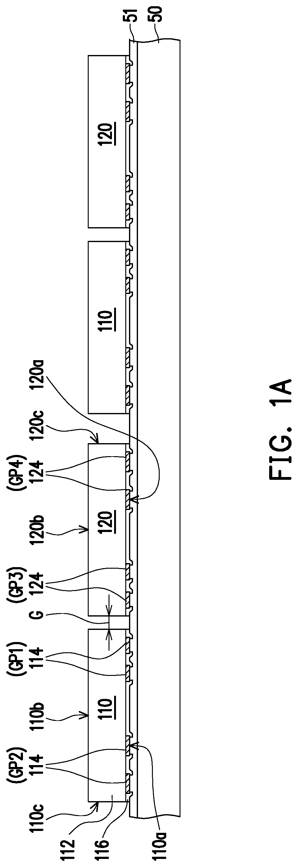
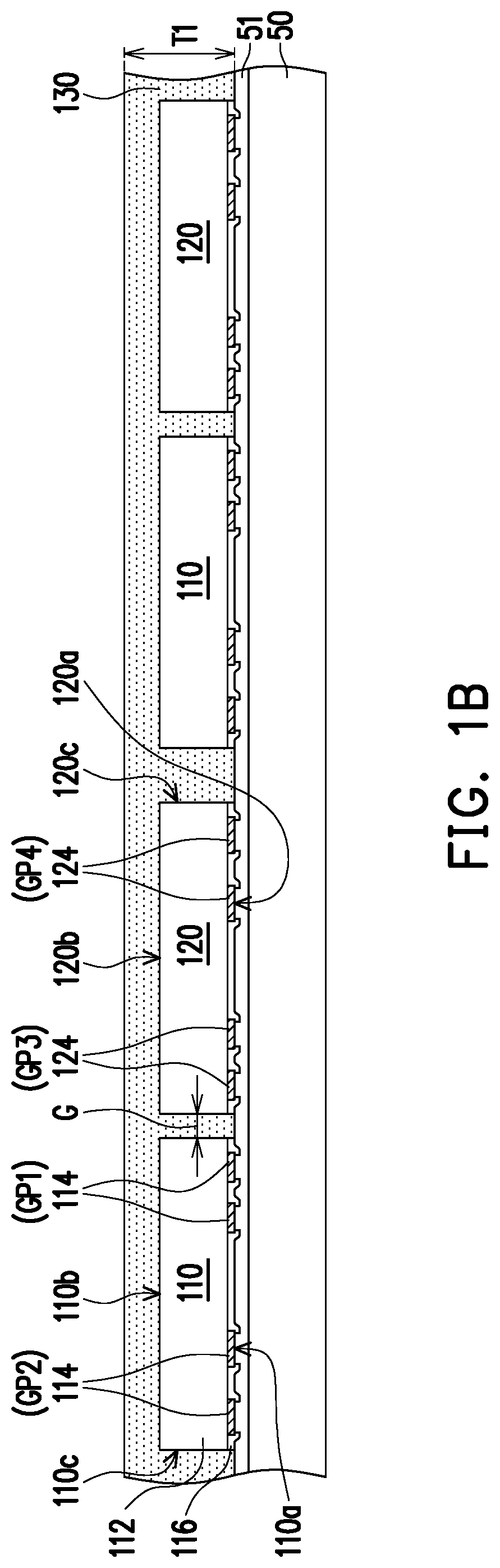
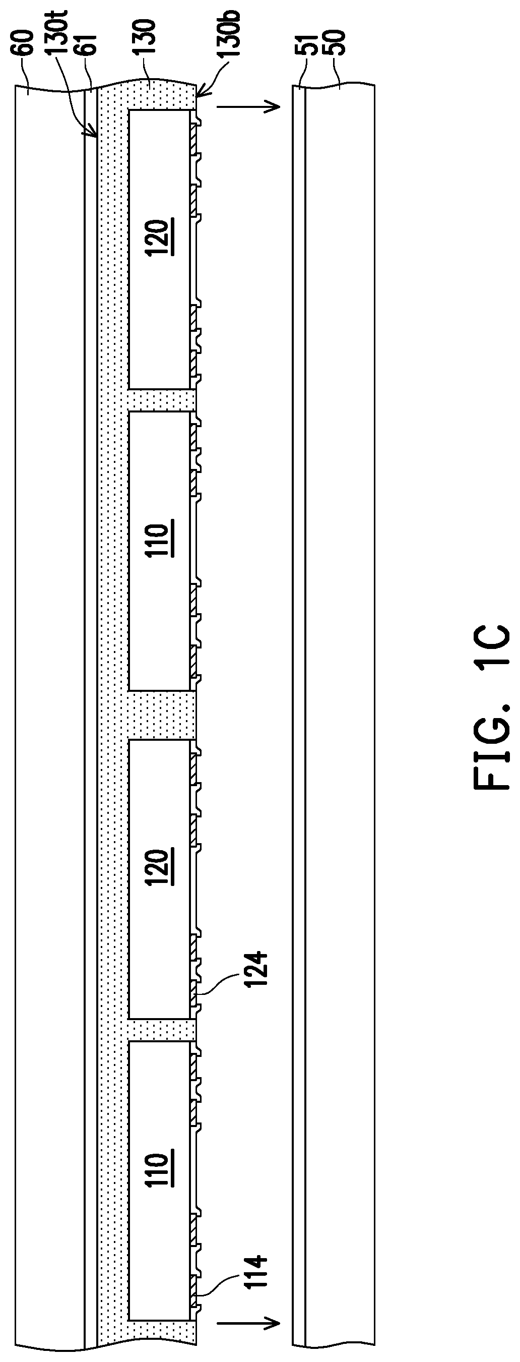
[0013]FIG. 1A to FIG. 1F are schematic cross-sectional views illustrating a manufacturing method of a semiconductor package according to an embodiment of the disclosure. Referring to FIG. 1A, a first active die 110 and a second active die 120 are disposed side by side over a temporary carrier 50. Throughout the description, the term “active die” may refer to a semiconductor die (or a semiconductor chip) having electrical function(s) that may contribute to the electrical operation of the resulting semiconductor package. The temporary carrier 50 may be a wafer-level or panel-level substrate made of glass, plastic, metal, or other suitable materials as long as the material is able to withstand the subs...


PUM

PropertyMeasurementUnit
distanceaaaaaaaaaa
conductiveaaaaaaaaaa
connecting lengthaaaaaaaaaa

Abstract

A semiconductor package and a manufacturing method thereof are provided. The semiconductor package includes a first and a second active dies separately arranged, an insulating encapsulation at least laterally encapsulating the first and the second active dies, a redistribution layer disposed on the insulating encapsulation, the first and the second active dies, and a fine-pitched die disposed on the redistribution layer and extending over a gap between the first and the second active dies. The fine-pitched die has a function different from the first and the second active dies. A die connector of the fine-pitched die is connected to a conductive feature of the first active die through a first conductive pathway of the redistribution layer. A first connecting length of the first conductive pathway is substantially equal to a shortest distance between the die connector of the fine-pitched die and the conductive feature of the first active die.

Description

CROSS-REFERENCE TO RELATED APPLICATION[0001]This application claims the priority benefit of U.S. provisional application Ser. No. 62 / 808,808, filed on Feb. 21, 2019. The entirety of the above-mentioned patent application is hereby incorporated by reference herein and made a part of this specification.BACKGROUND OF THE INVENTIONField of Invention[0002]The present invention generally relates to a package structure and a manufacturing method thereof, and more particularly, to a fan-out semiconductor package and a manufacturing method thereof.Description of Related Art[0003]In recently years, electronic apparatus are more important for human's life. In order for electronic apparatus design to achieve being light, slim, short, and small, semiconductor packaging technology has kept progressing, in attempt to develop products that are smaller in volume, lighter in weight, higher in integration, and more competitive in market. Since the chip package technique is highly influenced by the dev...

Claims


Application Information

Patent Timeline
Patent Type & Authority Applications(United States)
IPC IPC(8): H01L23/538H01L25/065H01L21/56H01L23/31
CPCH01L2224/04105H01L21/56H01L23/3107H01L23/5386H01L25/0655H01L23/5384H01L23/5385H01L23/5389H01L25/0652H01L24/26H01L23/49816H01L21/561H01L21/6835H01L2221/68359H01L2221/68345H01L24/96H01L24/19H01L2224/12105H01L2224/97H01L2224/73204H01L2224/32225H01L2224/16227H01L2924/19105H01L2224/81815H01L24/20H01L2224/16237H01L2224/81H01L2224/83H01L2224/16225H01L2924/00H01L24/09H01L23/293H01L2224/02372H01L21/565H01L21/76877H01L21/76816H01L23/5226
Inventor HSU, HUNG-HSINLIN, NAN-CHUNCHANG CHIEN, SHANG-YU
Owner POWERTECH TECHNOLOGY
Why Eureka
Try Eureka