Semiconductor package and manufacturing method thereof

a technology of semiconductor devices and packaging, applied in the direction of semiconductor devices, semiconductor/solid-state device details, electrical apparatus, etc., to achieve the effect of improving electrical performance and increasing manufacturability

Active Publication Date: 2020-08-27
POWERTECH TECHNOLOGY
View PDF4 Cites 4 Cited by
  • Summary
  • Abstract
  • Description
  • Claims
  • Application Information

AI Technical Summary

Benefits of technology

[0004]The disclosure provides a semiconductor package and a manufacturing method there

Problems solved by technology

Since the semiconductor package technique is highly influenced by the development of integrated circuits, therefore, as the size of electronics has become demanding, so does the package technique.
As

Method used


Image

  • Semiconductor package and manufacturing method thereof
  • Semiconductor package and manufacturing method thereof
  • Semiconductor package and manufacturing method thereof

Examples


Embodiment Construction

[0018]Reference will now be made in detail to the present preferred embodiments of the disclosure, examples of which are illustrated in the accompanying drawings. Wherever possible, the same reference numbers are used in the drawings and the description to refer to the same or like parts.

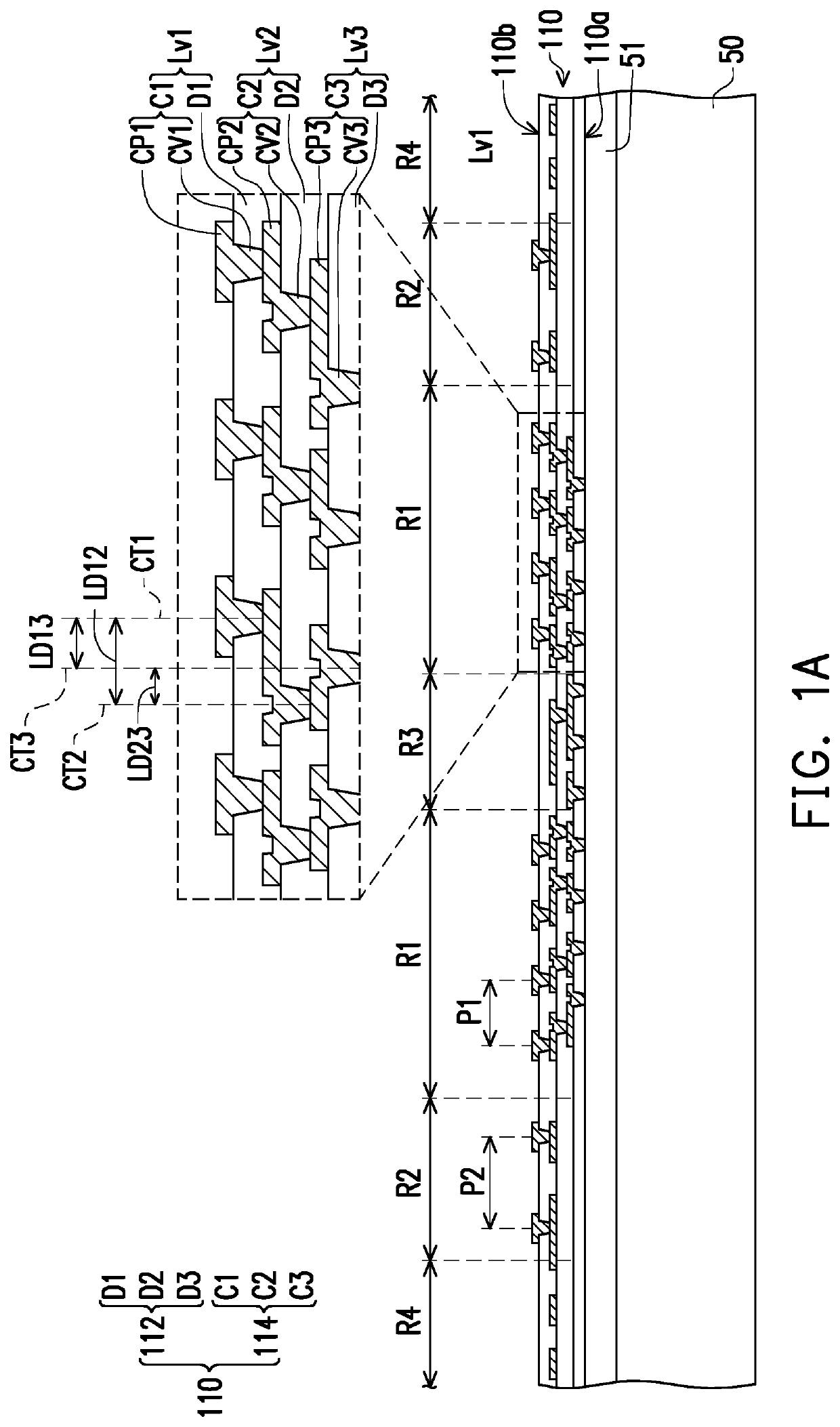
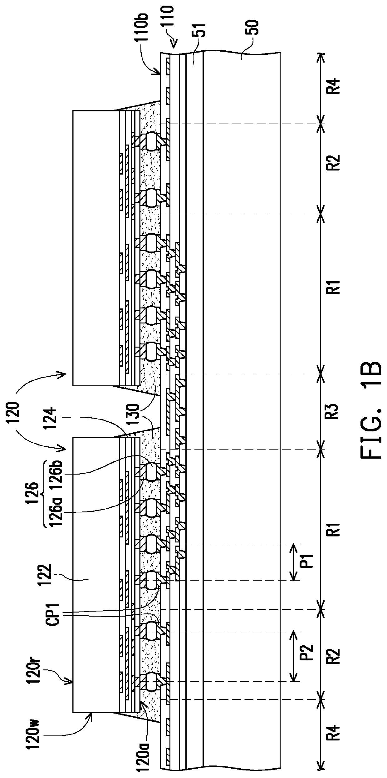
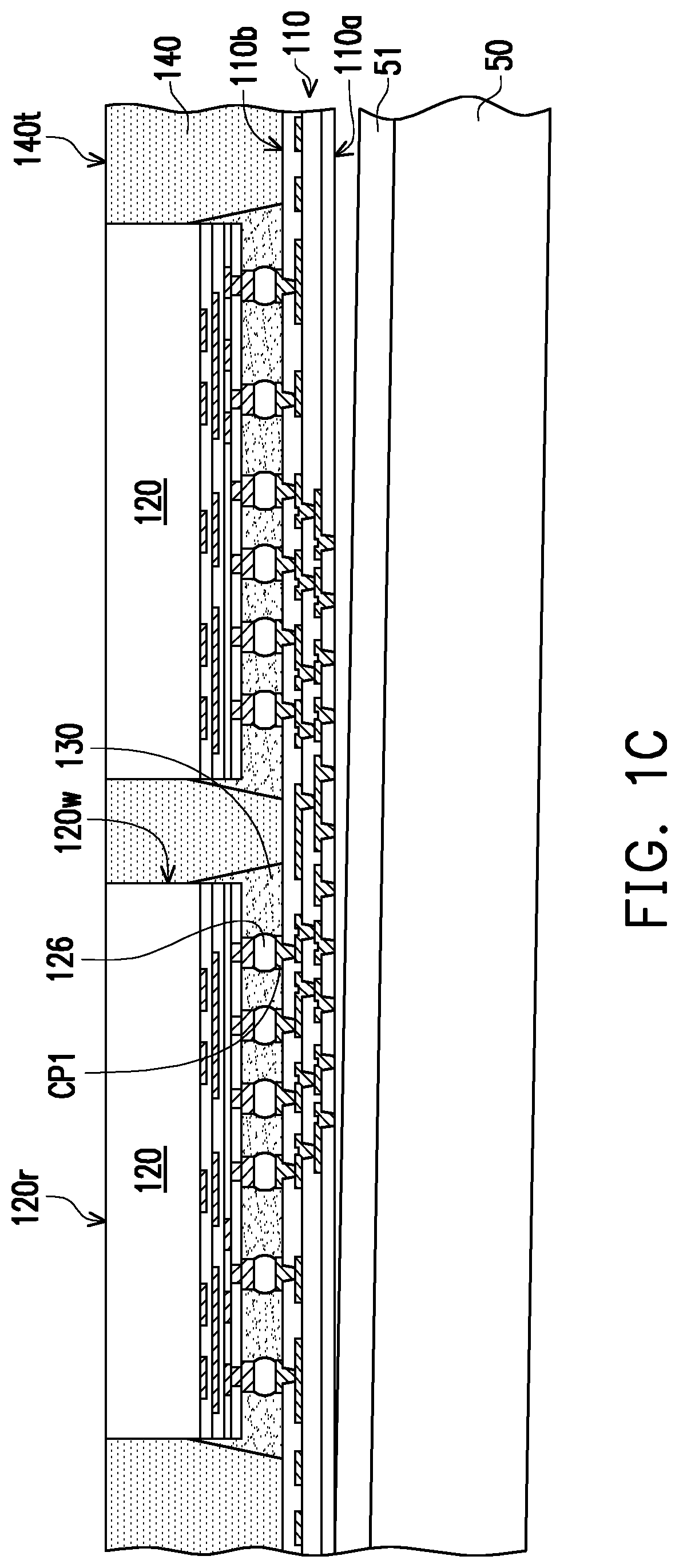
[0019]FIG. 1A to FIG. 1F are schematic cross-sectional views illustrating a manufacturing method of a semiconductor package according to an embodiment of the disclosure. Referring to FIG. 1A, a redistribution structure 110 is formed over a temporary carrier 50. For example, the temporary carrier 50 may be a wafer-level or panel-level substrate made of glass, plastic, metal, or other suitable materials as long as the material is able to withstand the subsequent processes while carrying the structure formed thereon. The redistribution structure 110 may include a first surface 110a facing towards the temporary carrier 50, and a second surface 110b opposite to the first surface 110a. In some embodiments...


PUM


Abstract

A semiconductor package and a manufacturing method thereof are provided. The semiconductor package includes first dies, an insulating encapsulation laterally encapsulating the first dies, a second die disposed over the portion of the insulating encapsulation and at least partially overlapping the first dies, and a redistribution structure disposed on the insulating encapsulation and electrically connected to the first dies and the second die. A second active surface of the second die faces toward first active surfaces of the first dies. The redistribution structure includes a first conductive via disposed proximal to the first dies, and a second conductive via disposed proximal to the second die. The first and second conductive vias are electrically coupled and disposed in a region of the redistribution structure between the second die and one of the first dies. The first conductive via is staggered from the second conductive via by a lateral offset.

Description

CROSS-REFERENCE TO RELATED APPLICATION[0001]This application claims the priority benefit of U.S. provisional application Ser. No. 62 / 808,808, filed on Feb. 21, 2019. The entirety of the above-mentioned patent application is hereby incorporated by reference herein and made a part of this specification.BACKGROUND OF THE INVENTIONField of Invention[0002]The present invention generally relates to a package structure and a manufacturing method thereof, and more particularly, to a semiconductor package including a bumpless die and a manufacturing method thereof.Description of Related Art[0003]In recently years, electronic apparatus are more important for human's life. In order for electronic apparatus design to achieve being light, slim, short, and small, semiconductor packaging technology has kept progressing, in attempt to develop products that are smaller in volume, lighter in weight, higher in integration, and more competitive in market. Since the semiconductor package technique is hi...

Claims


Application Information

Patent Timeline
IPC IPC(8): H01L23/00H01L23/29H01L23/31H01L23/522H01L21/56H01L21/768
CPCH01L23/293H01L2224/02372H01L21/76816H01L24/09H01L21/76877H01L23/5226H01L21/565H01L23/3107H01L25/0652H01L21/56H01L23/5386H01L24/26H01L23/5389H01L2224/04105H01L23/49816H01L21/561H01L21/6835H01L2221/68359H01L2221/68345H01L24/96H01L24/19H01L2224/12105H01L2224/97H01L2224/73204H01L2224/32225H01L2224/16227H01L2924/19105H01L2224/81815H01L24/20H01L2224/16237H01L2224/81H01L2224/83H01L2224/16225H01L2924/00H01L23/5384H01L23/5385H01L25/0655
Inventor HSU, HUNG-HSINCHANG CHIEN, SHANG-YULIN, NAN-CHUN
Owner POWERTECH TECHNOLOGY
Why Eureka
Try Eureka