Double-gate field-effect-transistor based biosensor

a biosensor and effect transistor technology, applied in the field of biosensors, can solve the problems of generating offset errors, requiring maintenance, and difficult miniaturisation, and achieve the effects of reducing manufacturing costs, easy miniaturisation, and reducing manufacturing costs

Active Publication Date: 2020-09-10
ECOLE POLYTECHNIQUE FEDERALE DE LAUSANNE (EPFL)
View PDF0 Cites 0 Cited by
  • Summary
  • Abstract
  • Description
  • Claims
  • Application Information

AI Technical Summary

Benefits of technology

[0006]The proposed new solution has the advantage that the sensor can be easily miniaturised and it is stable, ie it does not need frequent calibrations. Furthermore, the sensor is inexpensive. This means that even if a large number of sensors is manufactured, the manufacturing costs can be kept low. Optionally, there is no need for a separate reference electrode contrary to the prior art solutions. This would further lower the manufacturing costs.

Problems solved by technology

However, any variation or drift in the long term of this potential (notably via oxidation reduction (redox) reactions with the chemical species of the solution) generates an offset error.
They are usually bulky (with a size of a pen), require maintenance and are difficult to miniaturise.
Especially smaller sized reference electrodes are unstable over time and require frequent recalibration.

Method used


Image

  • Double-gate field-effect-transistor based biosensor
  • Double-gate field-effect-transistor based biosensor
  • Double-gate field-effect-transistor based biosensor

Examples


first embodiment

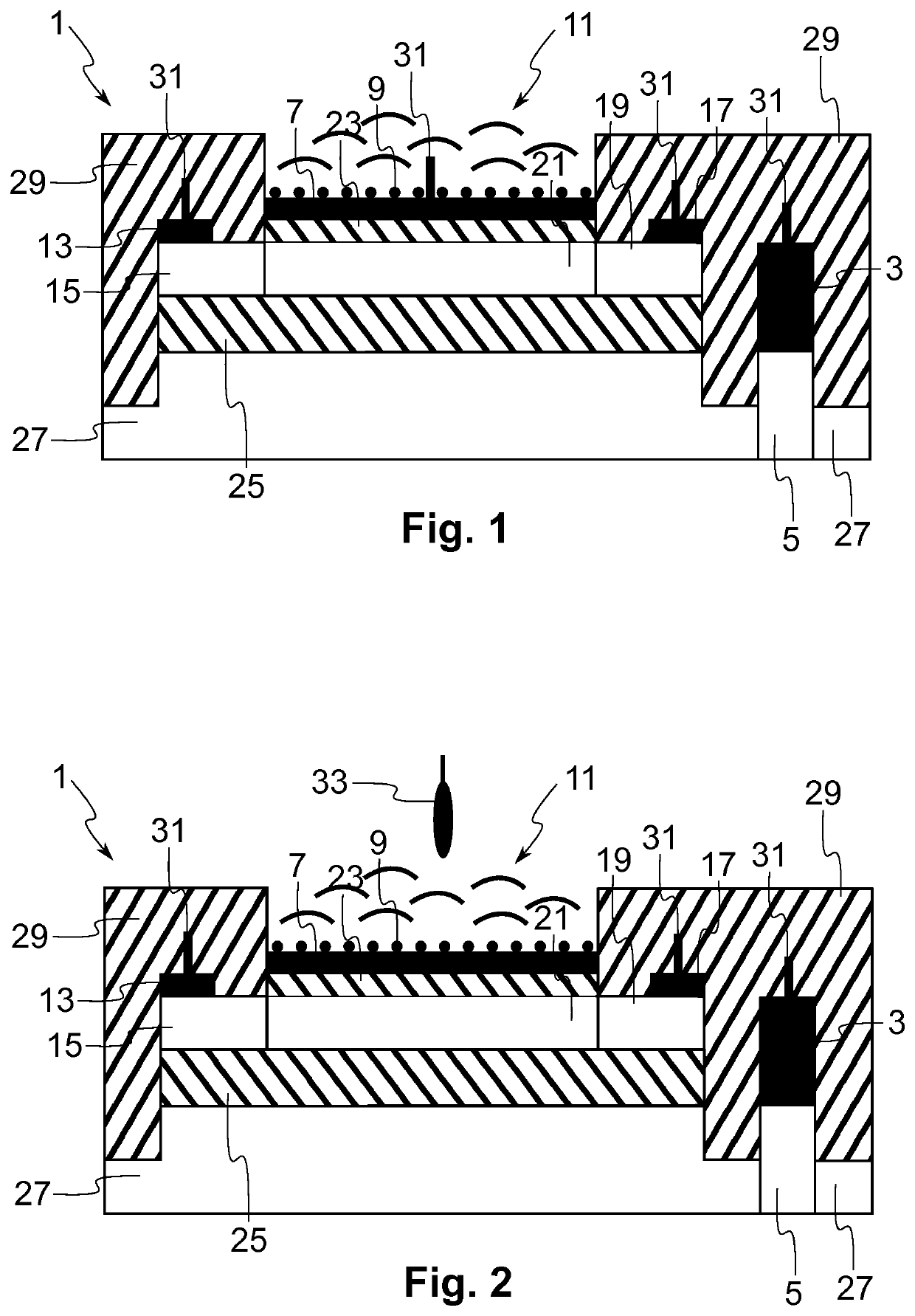
[0018]FIG. 1 is a schematic cross-section view of a multi-gate sensor 1, also referred to as a device, comprising two physically independent or separate gates according to the present invention. In the present description, by a multi-gate device is understood a device comprising at least two gate elements, nodes, terminals or regions. Thus, the device of FIG. 1 could comprise more than two gates. The biosensor 1 of FIG. 1 comprises a field-effect transistor (FET) exposed to a liquid solution. As can be seen in FIG. 1, the transistor comprises a first gate element, referred to as a back gate, comprising a back gate electrode 3 or electrical contact and a back gate doped region 5 in direct contact with the back gate electrode 3. The transistor also comprises a second gate element, referred to as a front gate, in this example comprising a front gate electrode 7 or electrical contact. In the present description, the electrical contacts are metal conductors, but they could instead be any...

third embodiment

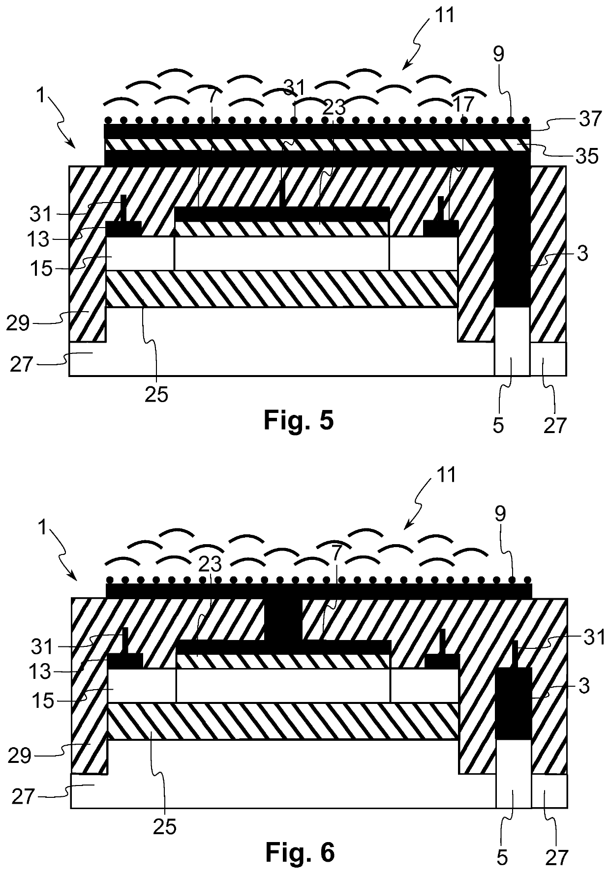
[0034]It is to be noted that the roles of the front and back gates may be inverted. In this case, the operating point of the transistor can be set via the source, drain and front gate biasing. The front gate coupling sets and controls the conductive channel between source and drain doped regions 15, 19 and the back gate stack is in contact with the solution 11. This is the present invention as shown in FIG. 3. It is to be noted that the electrical contact 3 of the back gate is usually not arranged via the back side (bottom) of the SOI substrate (due to the thickness of the base silicon and the parasitics notably) but it is arranged through the front (top) side as is the case also in the configuration of FIG. 3. During the fabrication process, a hole is etched through the BOX layer 25 of the SOI substrate in the location where the back gate contact should be placed and a (metal) plug contact is then formed to provide the electrical contact 3. Such a plug contact to the back gate may ...


PUM

PropertyMeasurementUnit
thicknessaaaaaaaaaa
thicknessaaaaaaaaaa
thicknessaaaaaaaaaa

Abstract

A biosensor includes a source element; a drain element; a semiconductor channel element between the source element and the drain element for forming an electrically conductive channel with adjustable conductivity between the source and drain elements; a first gate element configured to be electrically biased to set a given operational regime of the sensor with given electrical conductivity of the channel; and a second gate element, physically separate from the first gate element, configured to contact a solution comprising analytes allowed to interact with a gate contact surface of the second gate element to generate a surface potential change dependent on the concentration of the analytes in the solution. The channel element is substantially fully depleted allowing the first and second gate elements to be electrostatically coupled such that the surface potential change at the second gate element is configured to modify the electrical conductivity of the channel.

Description

TECHNICAL FIELD[0001]The present invention relates to a biosensor, such as an ion-sensitive field-effect transistor (ISFET), chemical field-effect transistor (ChemFET) or field-effect transistor-based biosensor (BioFET). The invention also relates to a fabrication method of the sensor.BACKGROUND OF THE INVENTION[0002]One of the first types of field-effect transistor biochemical sensors, ion-sensitive field-effect transistors, were first introduced by Bergveld in the early 70s. They provided a semiconductor alternative to the glass electrodes for pH and ion measurements. In its simplest form, an ISFET is comparable to a planar a metal-oxide-semiconductor field-effect transistor (MOSFET) except that the gate electrode directly in contact with the gate dielectric is instead replaced by a reference electrode acting as a local gate immersed in a solution contacting the gate dielectric. Alternatively, a metal layer and / or a functionalisation layer may cover (fully or partially) the gate d...

Claims


Application Information

Patent Timeline
Patent Type & Authority Applications(United States)
IPC IPC(8): G01N27/414
CPCG01N27/4145G01N27/414
Inventor IONESCU, MIHAI ADRIANGUERIN, HOËL
Owner ECOLE POLYTECHNIQUE FEDERALE DE LAUSANNE (EPFL)
Why Eureka
Try Eureka