Dopant enhanced solar cell and method of manufacturing thereof

a solar cell and dopant technology, applied in the direction of sustainable manufacturing/processing, climate sustainability, semiconductor devices, etc., can solve the problems of positive affecting the efficiency of the solar cell, achieve the effect of limiting recombination, improving compatibility, and reducing costs

Pending Publication Date: 2020-09-10
NEDERLANDSE ORG VOOR TOEGEPAST-NATUURWETENSCHAPPELIJK ONDERZOEK (TNO)
View PDF6 Cites 0 Cited by
  • Summary
  • Abstract
  • Description
  • Claims
  • Application Information

AI Technical Summary

Benefits of technology

[0008]The presence of this doping profile in the silicon substrate limits the recombination at the location of the metal contacts without requiring high polySi layer thicknesses and thus positively affects efficiency of the solar cell.
[0009]In a further embodiment the polysilicon layer is provided with a second dopant species of the first conductivity type having a dopant level in the polysilicon layer above the maximal dopant level in the silicon substrate. As a result, a positive differential exists across the thin oxide (or tunnel oxide) layer, creating “pull”, which ensures good transmission of charge carriers of the first conductivity type across the tunnel oxide layer from the silicon substrate towards the polysilicon layer. As a result, the efficiency of the solar cell is increased.
[0012]In an embodiment, the metal contacts are based on a fire-through metal paste. It is generally accepted that FT contacting technology is a well-established and low-cost technology, thus use of such contacts in the present invention provide better compatibility with present industrial manufacturing and lower costs. Additional advantage of FT contact technology is that it includes application of hydrogen-rich dielectric coating, which could be selected from PECVD SiNx:H and AL2O3, and so-called “firing”, which results in hydrogenation of the polySi / oxide stack, thereby favourably increasing the passivation performance of the layer stack. Due to the specific doping profile of the layer stack including dopant profile tail, the application of FT contacts on these doped polySi / oxide stacks only has very limited resulting recombination at the location of the interface, also when at some points metal is in direct contact with the silicon wafer (i.e., even without separating layer of interfacial oxide or polySi between the metal and wafer). Thus the combination of the doping profile throughout the stack and the use of FT contacts results in a desirably efficient solar cell with low manufacturing cost.

Problems solved by technology

The presence of this doping profile in the silicon substrate limits the recombination at the location of the metal contacts without requiring high polySi layer thicknesses and thus positively affects efficiency of the solar cell.

Method used


Image

  • Dopant enhanced solar cell and method of manufacturing thereof
  • Dopant enhanced solar cell and method of manufacturing thereof
  • Dopant enhanced solar cell and method of manufacturing thereof

Examples


Embodiment Construction

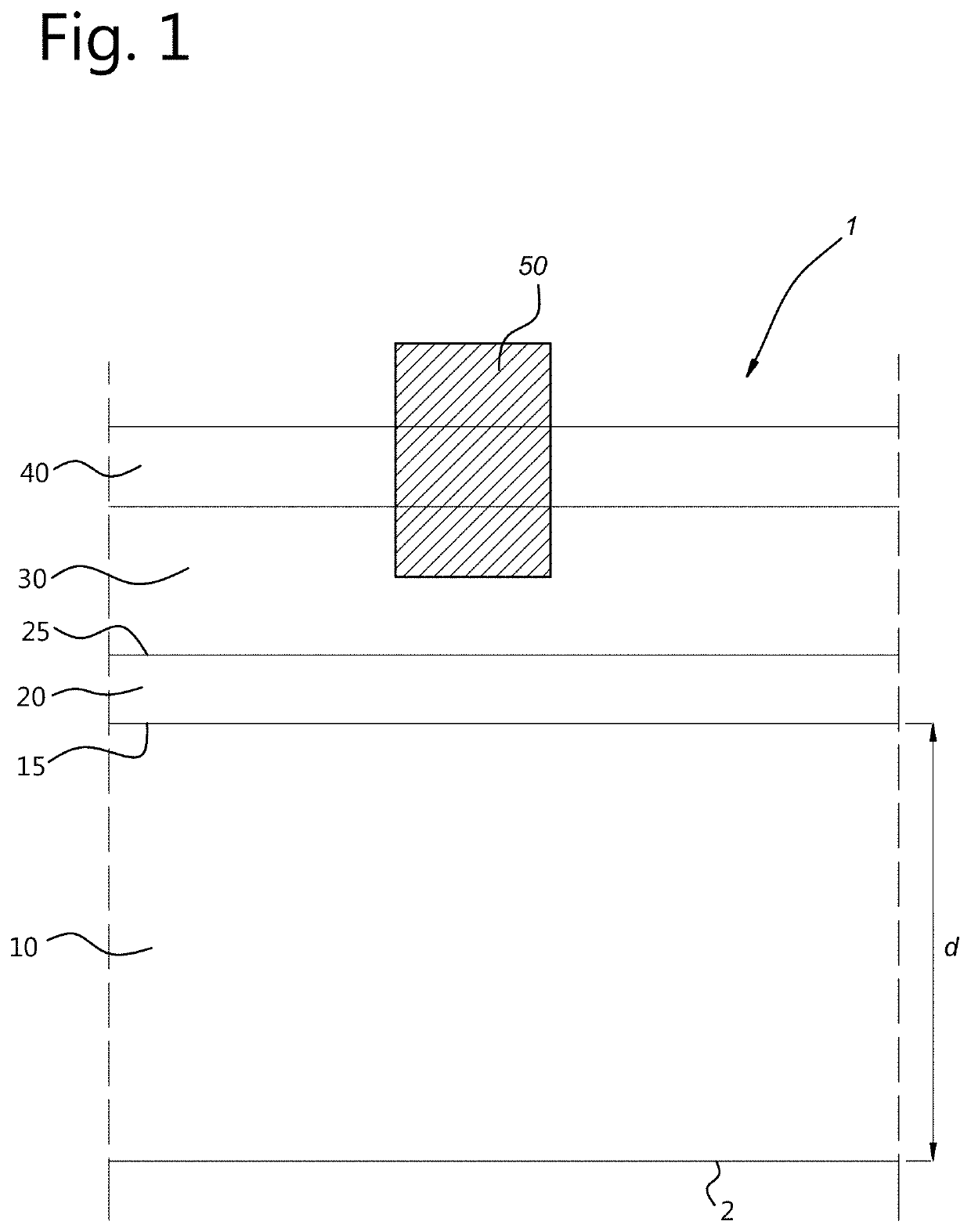
[0019]FIG. 1 depicts a cross-section of a polysilicon passivated solar cell with a metal contact. The solar cell layer stack 1 comprises a silicon substrate 10, a tunnel oxide layer 20, a polysilicon layer 30, an dielectric coating layer 40 and a metal contact 50.

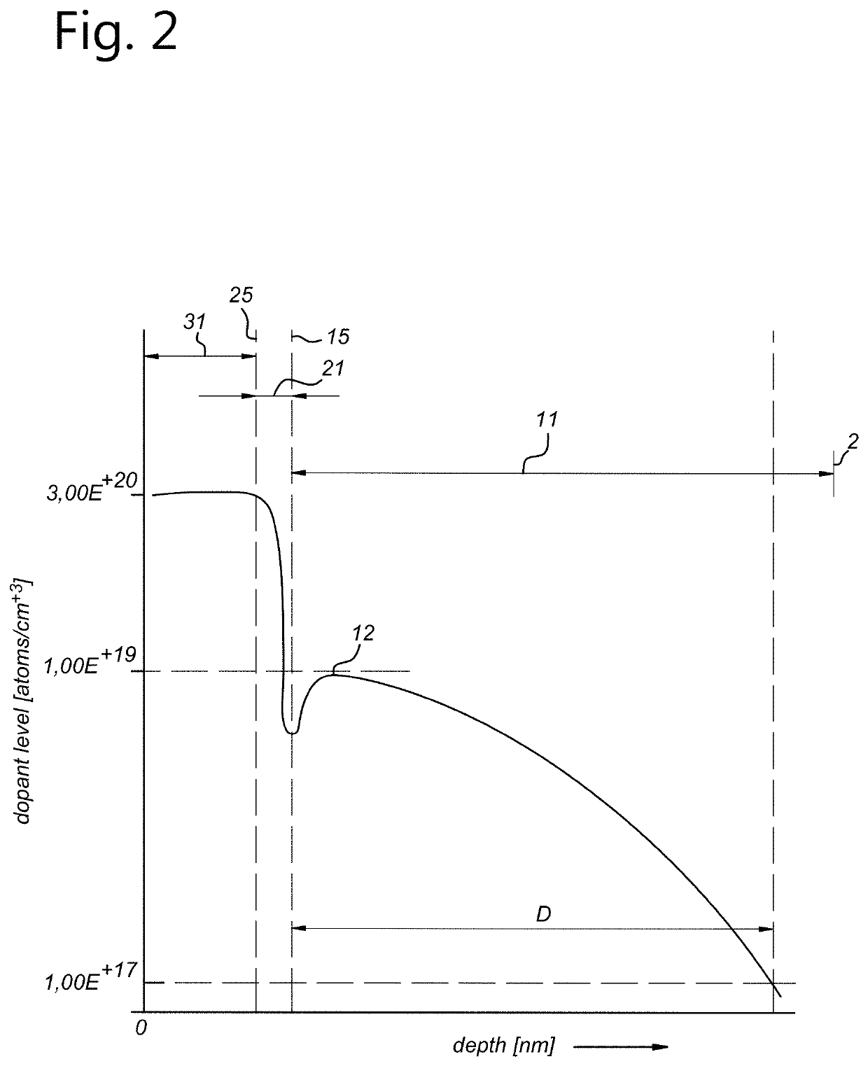
The silicon substrate 10 has a front surface 2, intended for facing the Sun when in use, and a rear surface onto which a tunnel oxide layer 20 has been created. A thin oxide is commonly used as tunnel oxide material. The layer has a minimum thickness of about 1 nm, 3 atomic layers, and is maximised at around 5 nm. The silicon substrate is a doped silicon wafer, which has been doped in a pre-diffusion step and / or during doping of polySi resulting in the claimed dopant profile which is discussed with reference to FIGS. 2 and 3. The thin oxide layer may be a silicon oxide or metal oxide and may contain other additional elements such as nitrogen. The thin oxide layer may in actual effect not be a perfect tunnel barrier, as it c...


PUM

PropertyMeasurementUnit
depthaaaaaaaaaa
depthaaaaaaaaaa
thicknessaaaaaaaaaa

Abstract

The present invention relates to a dopant enhanced silicon based solar cell and method of manufacturing thereof. The solar cell includes on a surface of the silicon substrate a layer stack including a thin oxide layer and a polysilicon layer, the thin oxide layer being arranged as a tunnel oxide layer in-between the surface of the substrate and the polysilicon layer. The solar cell is provided with fire-through metal contacts arranged on the layer stack locally penetrating into the polysilicon layer. The silicon substrate is provided at the side of the surface with a dopant species that creates a dopant profile of a first conductivity type in the silicon substrate. The dopant profile in the silicon substrate has a maximal dopant level between about 1×10+18 and about 3×10+19 atoms / cm3 and a depth of at least 200 nm within the substrate to a dopant atom level of 1×10+17 atoms / cm3.

Description

FIELD OF THE INVENTION[0001]The present invention relates to a dopant enhanced solar cell based on a silicon substrate and method of manufacturing thereof.BACKGROUND ART[0002]Doped polysilicon / thin oxide layer stacks (hereafter doped polySi / oxide stacks) can be used to form very high quality carrier-selective junctions for crystalline silicon cells, resulting in potentially very high cell efficiency. For contacting of the doped polysilicon (polySi) layer there are various options, such as fire-through (FT) paste, non-fire-through (NFT) paste, evaporated (PVD) metal, plated contacts and transparent conductive oxide (TCO).[0003]A limiting effect on cell efficiency are recombination losses, which can occur at various locations throughout the stack, whereby current is lost between the solar power collecting surface and the contact.[0004]Most preferred and therefore dominantly used contacts are FT contacts, i.e. contacts based on a FT paste, due to their low-cost and established technolo...

Claims


Application Information

Patent Timeline
Patent Type & Authority Applications(United States)
IPC IPC(8): H01L31/0224H01L31/18
CPCH01L31/02245H01L31/182H01L31/1864H01L31/022425H01L31/0745H01L31/1804Y02E10/546Y02E10/547Y02P70/50
Inventor STODOLNY, MACIEJ KRZYSZTOANKER, JOHNKOPPES, MARTIENROMIJN, INGRID GERDINAGEERLIGS, LAMBERT JOHAN
Owner NEDERLANDSE ORG VOOR TOEGEPAST-NATUURWETENSCHAPPELIJK ONDERZOEK (TNO)
Why Eureka
Try Eureka