MEMS Package, MEMS Microphone and Method of Manufacturing the MEMS Package
Active Publication Date: 2020-09-24
SAE MAGNETICS (HK) LTD
View PDF0 Cites 0 Cited by
Summary
Abstract
Description
Claims
Application Information
AI Technical Summary
This helps you quickly interpret patents by identifying the three key elements:
Problems solved by technology
Method used
Benefits of technology
Benefits of technology
The present invention is aimed at improving the strength and adhesion of thin-film filters used in MEMS packages and microphones. The solution is to enhance the strength of the films by increasing their thickness and forming micro perforations in them. This results in a filter that can prevent the entry of particles, water, and other substances that may damage the MEMS microphone. The invention also provides a method for manufacturing the MEMS package with these improved filters.
Problems solved by technology
However, because the conventional polymer film and processed film are formed in thin-film like shapes, having a very thin thickness, the films themselves are weak in the strength.
In that case, because the films are formed in thin-film like shapes, the parts, which are related to the adhesion or the like, are weak in the strength, therefore the films are likely to peel off.
However, if the thickness of the micro perforations-formed films is enlarged, the vibration of the air is weakened largely by the micro perforations-formed films, in accordance with the enlargement of the thickness.
Method used
Image
Click on the blue label to locate the original text in one second.
Reading with bidirectional positioning of images and text.
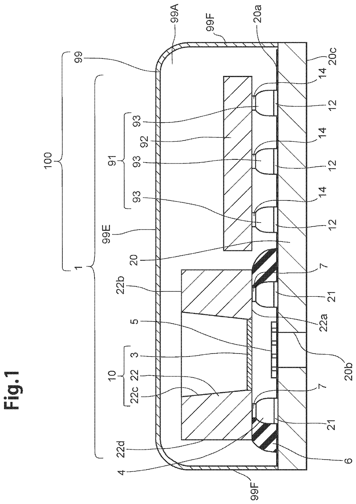
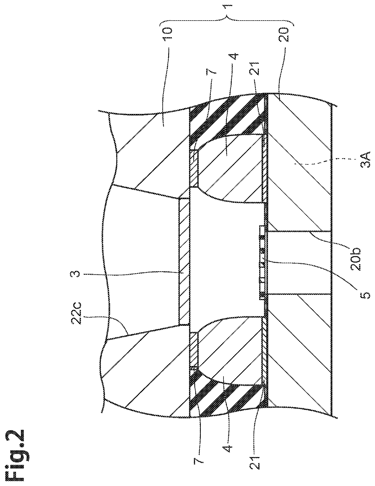
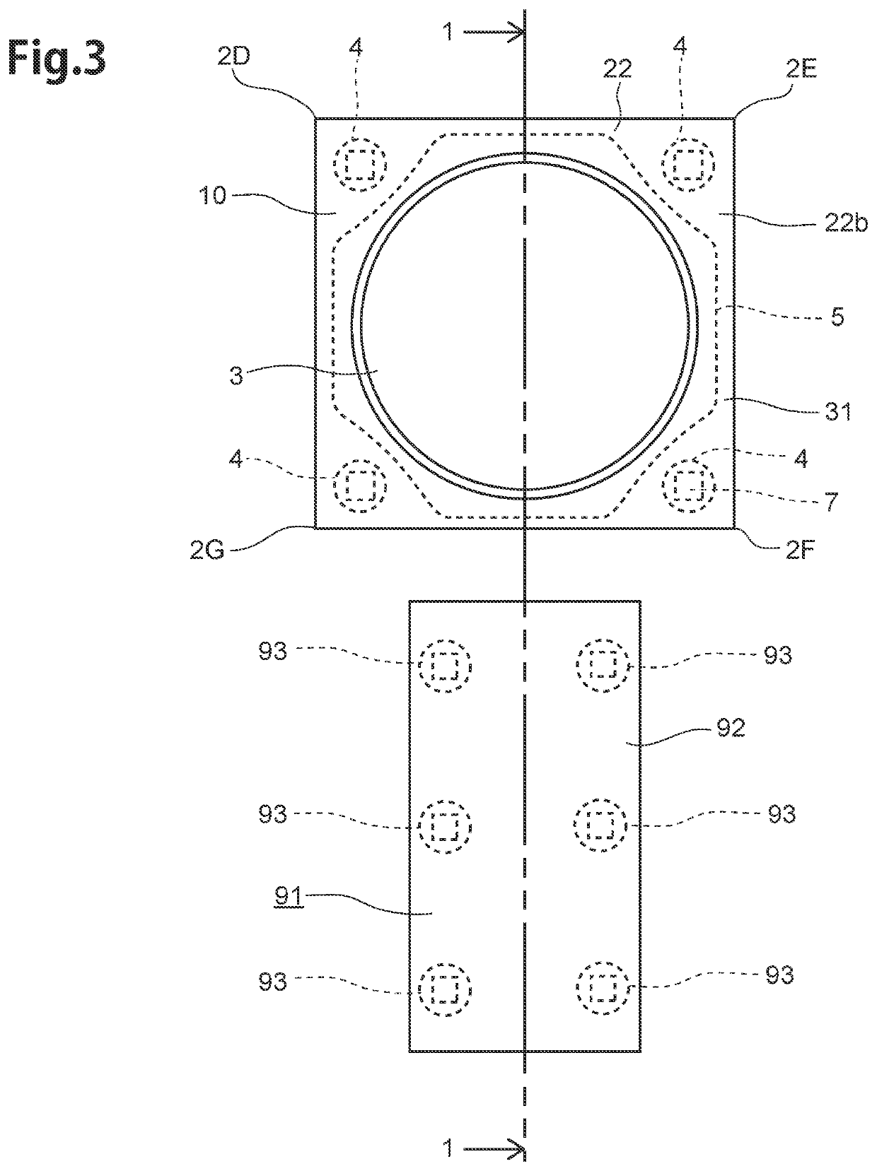
[0076]To begin with, the structures of the MEMS package 1 and the MEMS microphone 100, according to the first embodiment of the present invention, will be explained with reference to FIG. 1 to FIG. 3. Here, FIG. 1 is a sectional view showing a part, corresponding to the line 1-1 in FIG. 3, of a MEMS microphone 100 according to the first embodiment of the present invention. FIG. 2 is a sectional view, with enlargement, showing a principal part of FIG. 1. FIG. 3 is a plan view showing a principal part of the MEMS microphone 100 which a cap 99 is removed.
[0077]As illustrated in FIG. 1, the MEMS microphone 100 has the MEMS package 1 and the cap 99.
[0078]The MEMS package 1 has the MEMS chip 10, the package substrate 20, which the MEMS chip 10 is adhered, bonding bumps 4, the thin-film filter 5 and a sound shield 6. Further, the MEMS package 1 has an ASIC (Application SpecificIntegrated Circuit) package 91. In case of the MEMS package 1...
[0180]Next, the MEMS package 101 and the MEMS microphone 200, according to the second embodiment of the present invention will be explained with reference to FIG. 33. FIG. 33 is a sectional view, corresponding to FIG. 1, showing the MEMS microphone 200.
[0181]As illustrated in FIG. 33, the MEMS microphone 200 has the MEMS package 101 and the cap 99.
[0182]In case of the above-described MEMS microphone 100 (the MEMS package 1), the MEMS chip 10 and the ASIC 92 are mounted on the package substrate 20 by the flip chip bonding.
[0183]To the contrary, in case of the MEMS microphone 200 (the MEMS package 101) according to the second embodiment, the MEMS chip 10 and the ASIC 92 are mounted on the package substrate 20 by the wire bonding.
[0184]Then, the MEMS package 101 is different in the following a), b), c), as compared with the MEMS package 1.[0185]a) The thin-film filter 5 is adhered to the MEMS chip 10.[0186]b) The MEMS package 10...
PUM
Property
Measurement
Unit
Fraction
aaaaa
aaaaa
Thickness
aaaaa
aaaaa
Adhesion strength
aaaaa
aaaaa
Abstract
A MEMS package includes a MEMS chip, a package substrate which the MEMS chip is adhered and a thin-film filter which is adhered to the package substrate or the MEMS chip. The thin-film filter includes a thin-film part having a film surface and a rear film surface arranged a rear side of the film surface, and a plurality of through holes being formed to penetrate the thin-film part from the film surface to the rear film surface. The through holes are formed in an adhesive region of the thin-film part. The adhesive region is adhered to the package substrate or the MEMS chip.
Description
CROSS REFERENCE TO RELATED APPLICATIONS[0001]The present application claims the benefit of Japanese Patent Application No. JP2019-054758 filed on Mar. 22, 2019. All the above are hereby incorporated by reference. the contents of which are incorporated herein by reference in their entirety.BACKGROUNDField of the Invention[0002]The present invention relates to a MEMS package which a MEMS chip, being used as a microphone, a sensor and so on, is mounted on a package substrate, a MEMS microphone having the MEMS package and method of manufacturing the MEMS package.Related Background Art[0003]A minute device, which is called MEMS (Micro Electro Mechanical Systems), is conventionally known. The MEMS is a device which a minute movable element and an electronic circuit are integrated on a substrate (which is also called element substrate) made of silicon and so on. Because the whole of MEMS is formed in a chip-like form, the MEMS is also called a MEMS chip, in the present invention. The MEMS ...
Claims
Application Information
Patent Timeline
Application Date:The date an application was filed.
Publication Date:The date a patent or application was officially published.
First Publication Date:The earliest publication date of a patent with the same application number.
Issue Date:Publication date of the patent grant document.
PCT Entry Date:The Entry date of PCT National Phase.
Estimated Expiry Date:The statutory expiry date of a patent right according to the Patent Law, and it is the longest term of protection that the patent right can achieve without the termination of the patent right due to other reasons(Term extension factor has been taken into account ).
Invalid Date:Actual expiry date is based on effective date or publication date of legal transaction data of invalid patent.

