

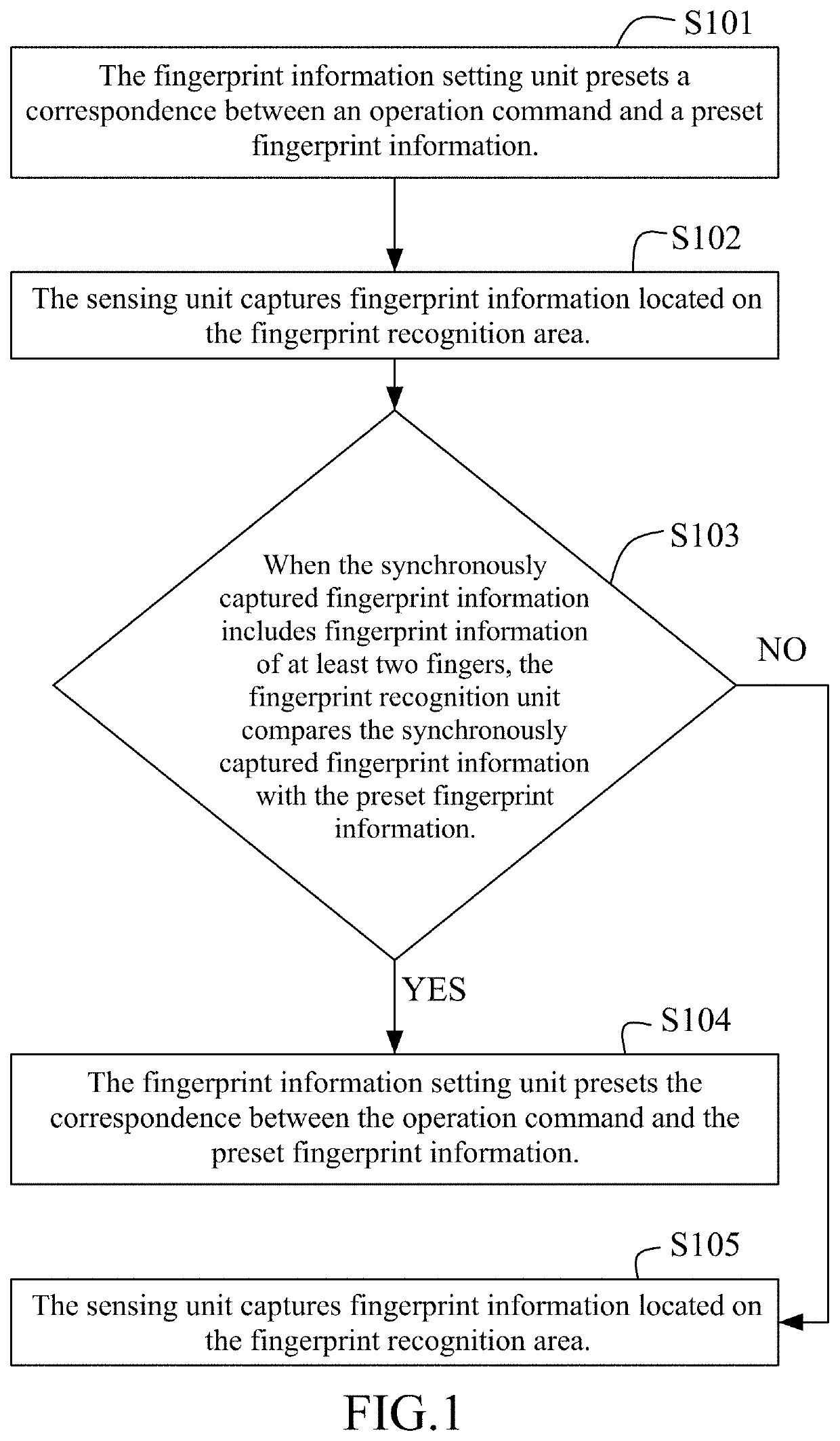
Fingerprint recognition based command execution method for electronic device, and electronic device
- Summary
- Abstract
- Description
- Claims
- Application Information
AI Technical Summary
Benefits of technology
Problems solved by technology
Method used
Image

Examples
second embodiment
[0195]In some embodiments, on the basis of the first or second embodiment, for each p-type / i-type / n-type structure, the p-type semiconductor layer may be a multilayer structure with more than two layers. For example, the p-type semiconductor layer is a three-layer structure which includes a first p-type semiconductor layer (p1 layer), a second p-type semiconductor layer (p2 layer), and a third p-type semiconductor layer (p3 layer) from top to bottom. The p1 layer can adopt an amorphous structure and be heavily doped with boron (the boron concentration is more than twice that of the standard process). The p2 and p3 adopt a microcrystalline structure and are normally doped with boron (doped in accordance with the standard process concentration). The absorption of light can be reduced by the thinner p2 and p3 layers, so that light enters the i-layer as much as possible and is absorbed by the i layer to improve photoelectric conversion rate. On the other hand, the p2 layer and the p3 la...
sixth embodiment
[0203]As shown in FIG. 8, it is a flowchart of an embodiment of a method for preparing light detection film of the present disclosure. The method is configured to prepare a photosensitive film transistor (i.e, a light detection film) of the sixth embodiment, and includes the following steps.
[0204]In a step S801, a gate is formed on the substrate of the pixel film transistor via magnetron sputtering. The substrate of the pixel film transistor can be a rigid board or a flexible material (such as polyimide) is executed
[0205]In a step S802, an insulating layer is deposited on the gate via chemical vapor deposition or magnetron sputtering.
[0206]In a step S803, an n-type doped semiconductor layer of the source and the drain is deposited on the insulating layer via chemical vapor deposition, and a metal layer of the source and the drain is deposited via magnetron sputtering, a preset structure of the source and the drain is defined via the yellow light etching process to make the source an...
fourth embodiment
[0209]In order to improve the photosensitive leakage current affected by the channel length between the source and the drain, so as to increase the area of the light-absorbing semiconductor without deteriorating the photoelectric conversion efficiency. In this embodiment, the source and the drain of the fourth embodiment are further improved, and a new structure of the source and the drain is proposed.
[0210]As shown in FIG. 4, the number of the source and drain are multiple. The sources are connected in parallel with each other, and the drain are connected in parallel with each other. The source and the drain are isolated by a gap. The photosensitive leakage current channel is formed between the source and drain laterally. The photosensitive leakage current channel includes a first gap formed between adjacent sources, a drain is placed in the first gap and a second gap formed between adjacent drains. The source and drain are arranged alternatively and isolated by a gap. The distance...
PUM
 Abstract
Description
Claims
Application Information