

Semiconductor device, semiconductor chip and method of manufacturing semiconductor device
- Summary
- Abstract
- Description
- Claims
- Application Information
AI Technical Summary
Benefits of technology
Problems solved by technology
Method used
Image

Examples
embodiment one
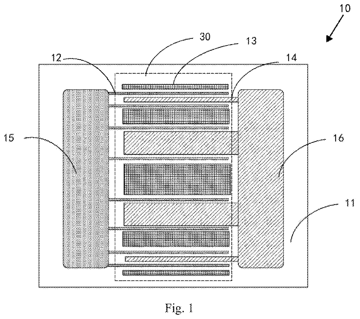
[0047]FIG. 1 is a top view of a semiconductor device provided by Embodiment one of the present disclosure. The semiconductor device 10 includes a substrate, a semiconductor layer 11, a plurality of gates 12, a plurality of drains 14, and a plurality of sources 13. The semiconductor layer 11 is located on one side of the substrate, and the plurality of gates 12, the plurality of drains 14, and the plurality of sources 13 are located on a side of the semiconductor layer 11 away from the substrate, the gates 12 are located between the sources 14 and the drains 13, and the plurality of gates 12, the plurality of drains 14, and the plurality of sources 13 are located in an active region 30 of the semiconductor device 10. Alternatively, the gate 12 may be, but not limited to, a stripe gate.
[0048]Further, during the use of the semiconductor device 10, since the position of the gate 12 is a region where the source leakage current and the electric field are concentrated and meanwhile is the ...
embodiment two
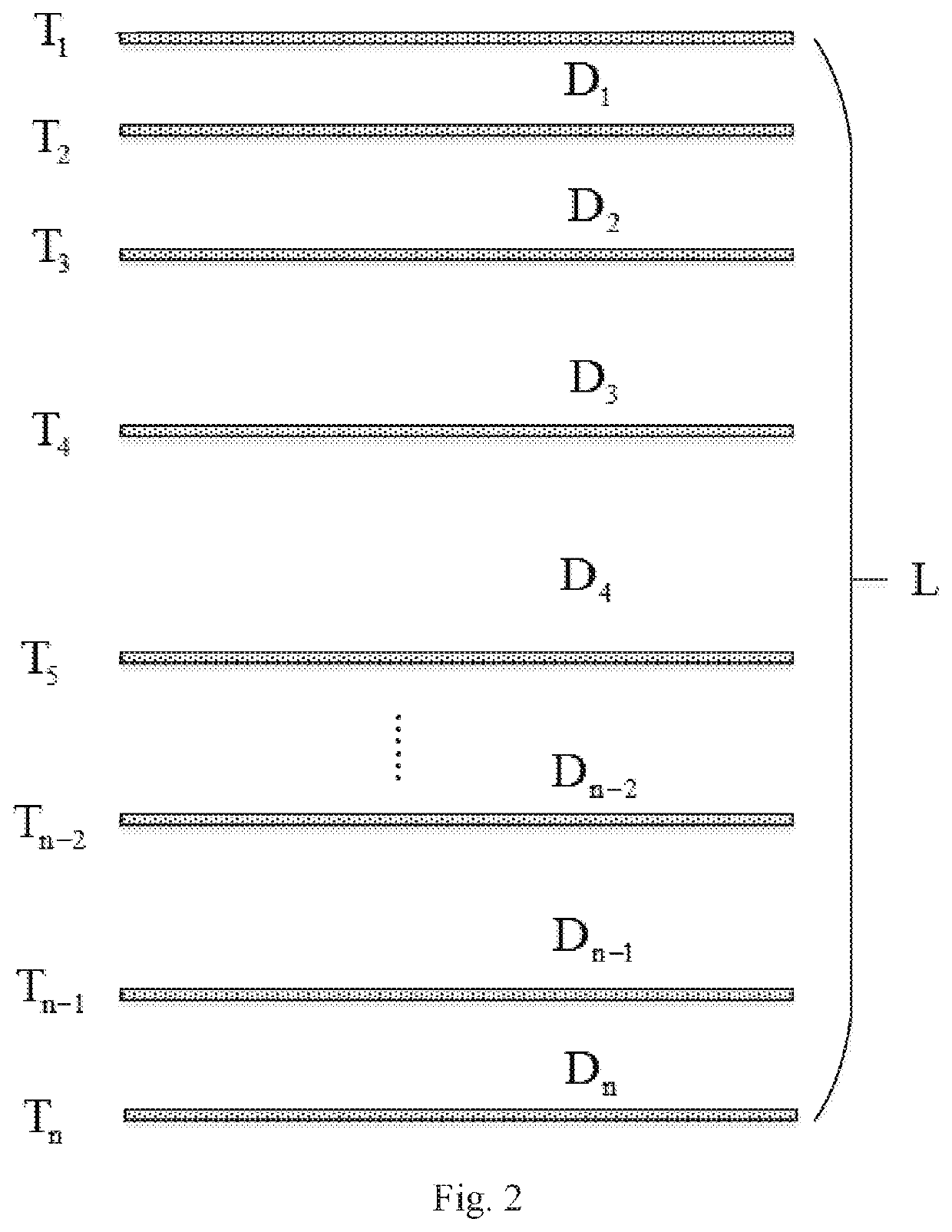
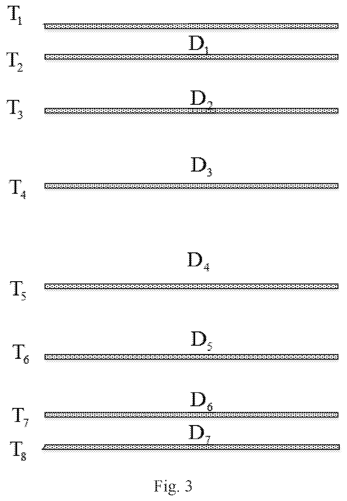
[0060]In order to reduce the inductance and parasitic capacitance of the device, the source 13 needs to be provided with a through hole; therefore, the gate pitches on both sides of the adjacent source 13 and drain 14 are different. As shown in FIG. 4, the gate finger pitch of both sides of the source 13 is d1, and the gate finger pitch of both sides of the drain 14 is d2, generally, the gate pitches d1 and d2 of both sides of the adjacent source 13 and drain 14 satisfy d2≤d1≤3d2. In order to reduce device losses and effectively balance the heat distribution, the maximum gate pitch is located at the center position of the active region 30, in a direction from the center position of the active region 30 to a position away from the center position, the respective pitches between adjacent gates 12 on both sides of the source 13 decrease sequentially according to a first fixed value or a first change amount, and the respective pitches between adjacent gates 12 on both sides of the drain...
embodiment three
[0061]Based on the design and description of the semiconductor device 10 given in Embodiment one, as shown in FIG. 5, Embodiment three of the present disclosure further provides a semiconductor chip 20 including a plurality of semiconductor devices 10, and the plurality of semiconductor devices 10 are connected in parallel. A gate pitch between devices is formed between edge gates 12 of any two adjacent semiconductor devices 10 of the semiconductor chip 20, and the gate pitches between devices decrease sequentially according to a third fixed value or a third change amount. The setting of the gate pitch between the semiconductor devices 10 in the semiconductor chip 20 can effectively alleviate the heat generation between the device edges and balance the heat distribution of the entire chip. It should be understood that the semiconductor device 10 given in this embodiment has the same structural features as the semiconductor device 10 described in Embodiment one, so this embodiment wi...
PUM
 Abstract
Description
Claims
Application Information