Subsurface inspection method and system

Inactive Publication Date: 2020-10-29
NEDERLANDSE ORG VOOR TOEGEPAST-NATUURWETENSCHAPPELIJK ONDERZOEK (TNO)
View PDF0 Cites 4 Cited by
  • Summary
  • Abstract
  • Description
  • Claims
  • Application Information

AI Technical Summary

Benefits of technology

[0035]A greater dispersion provided by the optic can result in an enhanced ‘separation’ of the reference laser beam and the laser probe beam since the velocity of the surface of the sample deflecting is taken into account, resulting in a greater phase difference at the optical interference detector. In this way, subsurface feature extraction can be improved. Op

Problems solved by technology

Overlay errors may for example occur as a result of interlayer misalignment between (functional) layers of a multilayer semiconductor device.
The term ‘overlay error’ relates to the amount of misalignment between subsequent layers, and therefore may include offset errors, i.e. errors in the position of a layer in relation to other layers, as well as layer alignment errors, i.e. incorrect orientation of a layer with respect to other layers.
When the acoustic wave is reflected back on a structure inside

Method used


Image

  • Subsurface inspection method and system
  • Subsurface inspection method and system
  • Subsurface inspection method and system

Examples


Example

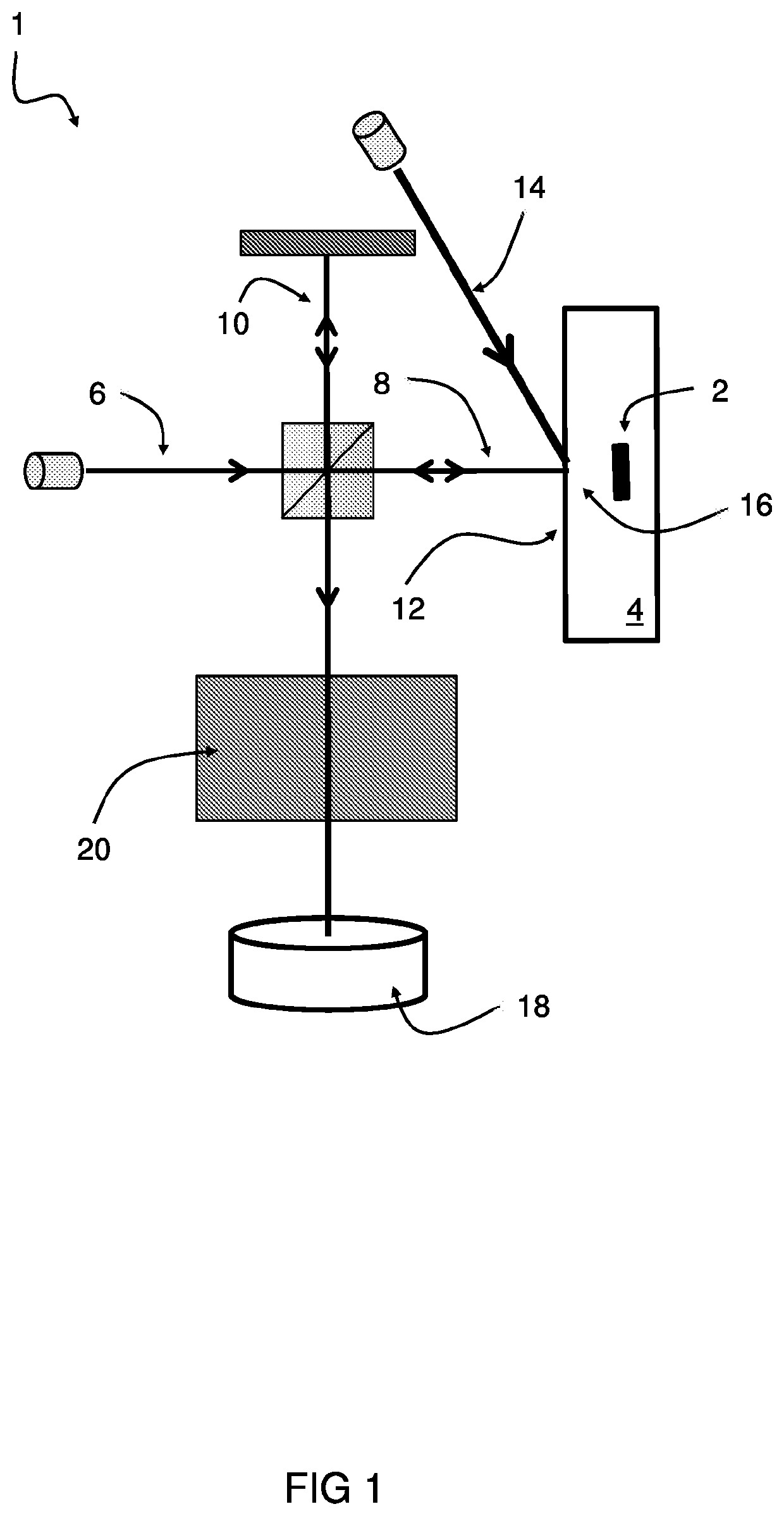
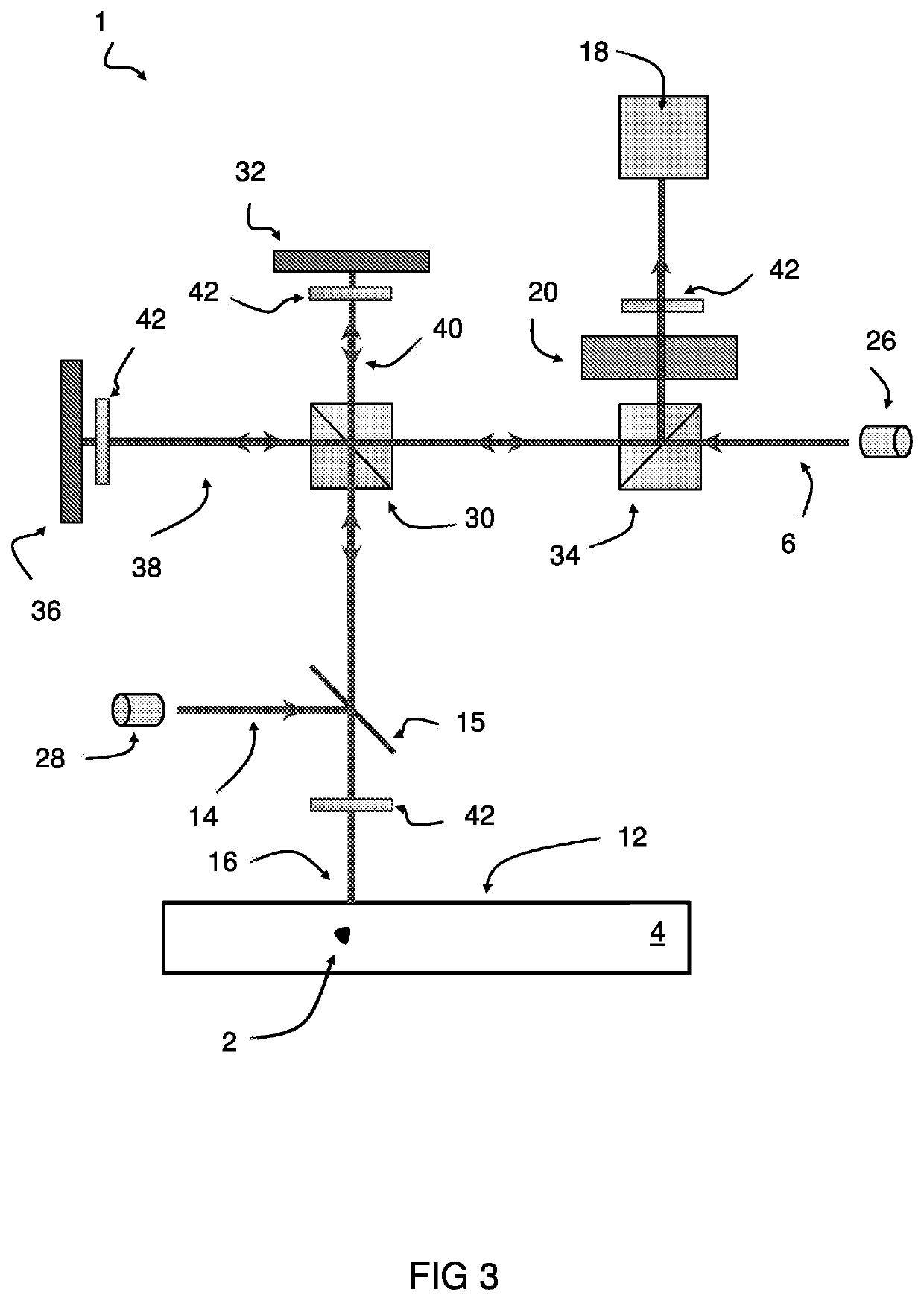
[0058]FIG. 1 shows a schematic diagram of an embodiment of a subsurface wafer inspection system 1. The method can be employed for identifying internal subsurface features, such as defects or anomalies 2 in a semiconductor wafer 4, and / or for identifying overlay or misalignment errors in the semiconductor wafer 4.

[0059]The system 1 comprises a laser interferometer having a controller configured to carry out the steps of: splitting a measurement laser beam 6 into a laser probe beam 8 and a reference laser beam 10; transmitting the laser probe beam 8 to a surface 12 of the wafer 4; transmitting a laser excitation pulse 14 impinging upon a target location 16 on the surface 12 of the wafer 4 to generate an ultrasound wave propagating through the wafer 4, wherein the ultrasound wave causes a wafer surface movement at or near the target location 16 when reflected back from an encountered subsurface feature, such as defect 2 inside the wafer 4; recombining the laser probe beam 8 and the ref...


PUM


Abstract

A subsurface inspection method and system (1) for detecting internal defects (2) and/or overlay/misalignment in a semiconductor wafer (4). A measurement laser beam (6) is split into a laser probe beam (8) and a reference laser beam (10). The laser probe beam is transmitted to a wafer surface (12). A laser excitation pulse (14) is transmitted impinging the wafer surface for causing an ultrasound wave propagating through the wafer and causing wafer surface movement when reflected back from an encountered subsurface feature. The laser probe beam and the reference laser beam are recombined in an optical interference detector (18) and the subsurface feature inside the wafer is detected by a deviation of a detected phase difference. The laser probe beam and the reference laser beam are guided through an optic (20) prior to arriving at the optical interference detector. The optic has a dispersive characteristic dimensioned to enlarge the phase difference between the reference beam and the wave length shifted probe beam.

Description

FIELD OF THE INVENTION[0001]The invention relates to a method and system for subsurface inspection.BACKGROUND TO THE INVENTION[0002]A wafer or semiconductor device may require regular inspections for internal (structural) defects, irregularities, or anomalies which may be present inside, for instance to ensure quality, integrity and / or reliability of the wafer. Such subsurface features can be invisible or hidden when for example performing known surface inspection methods. Subsurface inspection or imaging may be required to examine subsurface domains of the wafer for the presence of inhomogeneities or the like, which may strongly influence the functionality, quality and / or the lifetime of the wafer.[0003]Also overlay error between device layers of for example a multilayer semiconductor device may need to be determined. Overlay errors may for example occur as a result of interlayer misalignment between (functional) layers of a multilayer semiconductor device. In the multilayered stru...

Claims


Application Information

Patent Timeline
IPC IPC(8): G01N29/24G01N29/04
CPCG01N2033/0095G01N2291/2697G01N29/043G01N29/2418G01B11/0666G01B11/2441G01B21/085G01N21/1717G01N21/9505G01N29/06G01N29/2437G01S15/8965G03F7/70633
Inventor KOEK, WOUTER DICKVAN ZWET, ERWIN JOHN
Owner NEDERLANDSE ORG VOOR TOEGEPAST-NATUURWETENSCHAPPELIJK ONDERZOEK (TNO)
Why Eureka
Try Eureka