Memory device

Active Publication Date: 2020-10-29
SEMICON ENERGY LAB CO LTD
View PDF0 Cites 2 Cited by
  • Summary
  • Abstract
  • Description
  • Claims
  • Application Information

AI Technical Summary

Benefits of technology

[0027]According to one embodiment of the present invention, a highly-integrated memory device can be provided. Alternatively, a memory device which is less likely to be affected by noise can be provided. Alternatively, a memory dev

Problems solved by technology

The twisted bit-line method can be employed in a folded bit-line memory device but cannot be employed in an open bit-line me

Method used


Image

  • Memory device
  • Memory device
  • Memory device

Examples


embodiment 1

[0066]A memory device of one embodiment of the present invention is described with reference to drawings.

[0067]First, a folded bit-line memory device and an open bit-line memory device are described.

[0068]FIG. 8A is a block diagram illustrating a folded bit-line memory device 901. The memory device 901 includes a cell array 921 including memory cells 911 arranged in a matrix, a plurality of word lines, a plurality of bit lines, and a plurality of sense amplifiers SA. In the memory device 901, the plurality of bit lines extend in the row direction (or in the column direction), and the plurality of word lines extend in the column direction (or in the row direction).

[0069]The plurality of word lines each intersect with a plurality of bit line pairs. The plurality of bit lines include a plurality of bit lines BL and a plurality of bit lines BLB. FIG. 8A illustrates three bit lines BL (bit lines BL1 to BL3) and three bit lines BLB (bit lines BLB1 to BLB3).

[0070]In the folded bit-line mem...

embodiment 2

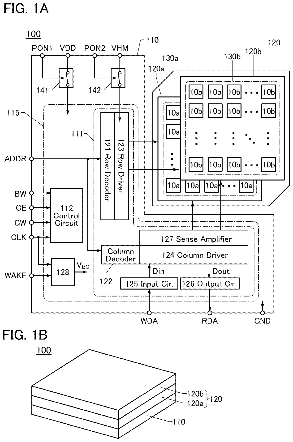
[0130]In this embodiment, cross-sectional structure examples of the memory device 100 and a memory device 100A are described with reference to drawings.

[0131]FIG. 10 illustrates a cross section of part of the memory device 100. The layer 110, the layer 120a, and the layer 120b are stacked over a substrate 231 in the memory device 100 illustrated in FIG. 10. FIG. 10 illustrates a case where a single crystal semiconductor substrate (e.g., a single crystal silicon substrate) is used as the substrate 231. A source, a drain, and a channel of a transistor in the layer 110 are formed in part of the substrate 231. The layer 120a and the layer 120b each include a thin film transistor (e.g., an ox transistor).

[Layer 110]

[0132]The layer 110 in FIG. 10 includes, over the substrate 231, a transistor 233a, a transistor 233b, and a transistor 233c. FIG. 10 illustrates cross sections of the transistor 233a, the transistor 233b, and the transistor 233c in the channel length direction.

[0133]Channels ...

modification example

[0152]FIG. 11 illustrates a cross section of part of a memory device 100A. The memory device 100A is a modification example of the memory device 100. The memory device 100A includes a layer 110A, the layer 120a, and the layer 120b. The layer 110A, the layer 120a, and the layer 120b are provided over the substrate 231 in this order. An insulating substrate (e.g., a glass substrate) is used as the substrate 231 of the memory device 100A.

[0153]The layer 110A includes a transistor 268a, a transistor 268b, and a capacitor 269a. A thin film transistor (e.g., an ox transistor) is used as each of the transistors in the layer 110A. The layer 120a and the layer 120b can be formed in a manner similar to those described above.

[0154]All the transistors in the layer 110A are ox transistors, whereby the layer 110A can be an integrated circuit in which all the transistors have the same conductivity. All the transistors in the memory device 100A are ox transistors, whereby the memory device 100A can...


PUM


Abstract

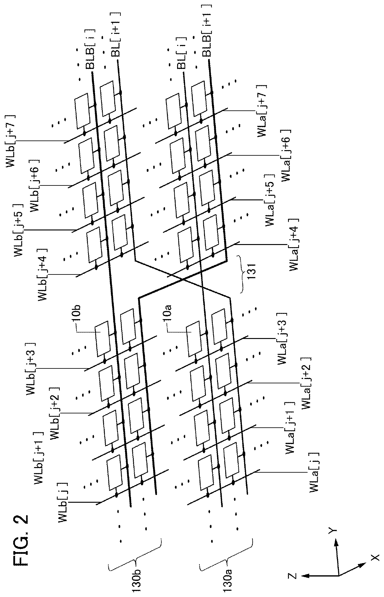
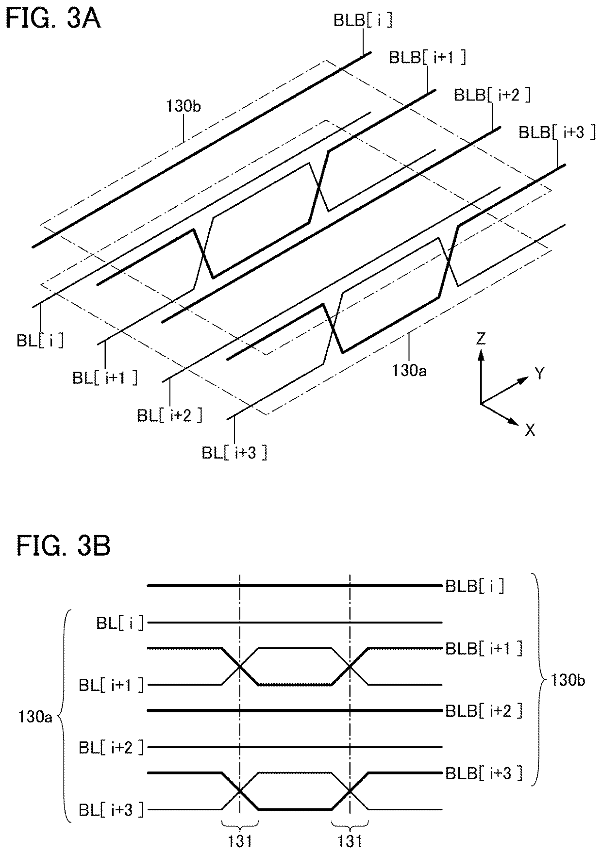
A novel memory device is provided. A first cell array including a plurality of memory cells and a second cell array including a plurality of memory cells are stacked. One of two bit lines of a first bit line pair is electrically connected to A memory cells of the first cell array, and the other of the two bit lines of the first bit line pair is electrically connected to D memory cells of the second cell array. One of two bit lines of a second bit line pair is electrically connected to B memory cells of the first cell array and F memory cells of the second cell array, and the other of the two bit lines of the second bit line pair is electrically connected to C memory cells of the first cell array and E memory cells of the second cell array. The first bit line pairs and the second bit line pairs are alternately provided.

Description

TECHNICAL FIELD[0001]One embodiment of the present invention relates to a memory device, a semiconductor device, or an electronic device including either of these devices.[0002]Note that one embodiment of the present invention is not limited to the above technical field. One embodiment of the invention disclosed in this specification and the like relates to an object, a method, or a manufacturing method. One embodiment of the invention disclosed in this specification and the like also relates to a process, a machine, manufacture, or a composition of matter.[0003]In this specification and the like, a semiconductor device generally means a device that can function by utilizing semiconductor characteristics. A transistor and a semiconductor circuit are embodiments of semiconductor devices. A display device (e.g., a liquid crystal display device and a light-emitting display device), a projection device, a lighting device, an electro-optical device, a power storage device, a memory devic...

Claims


Application Information

Patent Timeline
IPC IPC(8): H01L27/105H01L27/12H01L29/786
CPCH01L27/1207H01L29/7869H01L29/78648H01L27/124H01L27/1255H01L27/1052H01L27/1225G11C7/18G11C11/4097G11C7/02G11C11/404G11C7/04H10B12/312H10B12/30H10B99/00
Inventor ONUKI, TATSUYAOKAMOTO, YUKIIKEDA, HISAONAGATSUKA, SHUHEI
Owner SEMICON ENERGY LAB CO LTD
Why Eureka
Try Eureka