
Photocatalytic electrode for water splitting and water splitting device

a photocatalytic electrode and water splitting technology, applied in the direction of electrolysis components, electrolysis coatings, physical/chemical process catalysts, etc., can solve the problems of insufficient onset potential and insatisfactory performance of water splitting devices, and achieve excellent onset potential

Inactive Publication Date: 2020-12-10
FUJIFILM CORP +1
View PDF0 Cites 5 Cited by
  • Summary
  • Abstract
  • Description
  • Claims
  • Application Information

AI Technical Summary

Benefits of technology

The present invention provides a photocatalytic electrode for water splitting and a water splitting device that have excellent onset potential. This is achieved by using a CIGS compound semiconductor with a specific molar ratio of Ga to the total amount of Ga and In. The invention also ensures that the band offset, which is the difference between the potential at the lower end of the conduction band of the p-type semiconductor layer and the potential at the lower end of the conduction band of the n-type semiconductor layer, is equal to or less than a predetermined value. Overall, this advancement improves the efficiency and performance of photocatalytic water splitting devices.

Problems solved by technology

From this viewpoint, the present inventors applied the CIGS compound semiconductor used for a solar battery, which is described in the above literature, to a photocatalytic electrode for water splitting, but the onset potential was insufficient and the performance required for a water splitting device was not satisfied.

Method used


Image

  • Photocatalytic electrode for water splitting and water splitting device
  • Photocatalytic electrode for water splitting and water splitting device

Examples


first embodiment

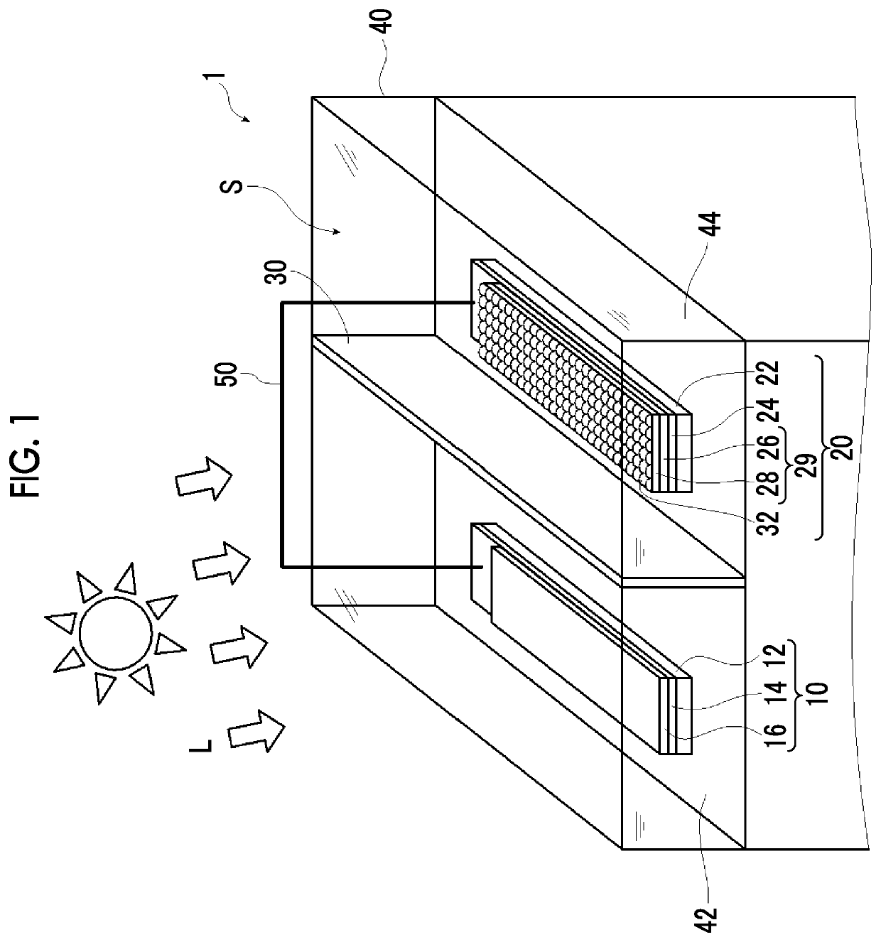
[0037]In one embodiment of a water splitting device of the present invention, the water splitting device generates gases from a photocatalytic electrode for hydrogen generation and a photocatalytic electrode for oxygen generation by irradiating the photocatalytic electrode for hydrogen generation and the photocatalytic electrode for oxygen generation with light, and includes a bath to be filled with an electrolytic aqueous solution and the photocatalytic electrode for hydrogen generation and the photocatalytic electrode for oxygen generation each disposed in the bath, in which the photocatalytic electrode for hydrogen generation has a p-type semiconductor layer, an n-type semiconductor layer provided on the p-type semiconductor layer, and a co-catalyst provided on the n-type semiconductor layer, the p-type semiconductor layer is a semiconductor layer containing a CIGS compound semiconductor containing Cu, In, Ga, and Se, and a molar ratio of Ga to a total molar amount of Ga and In i...

second embodiment

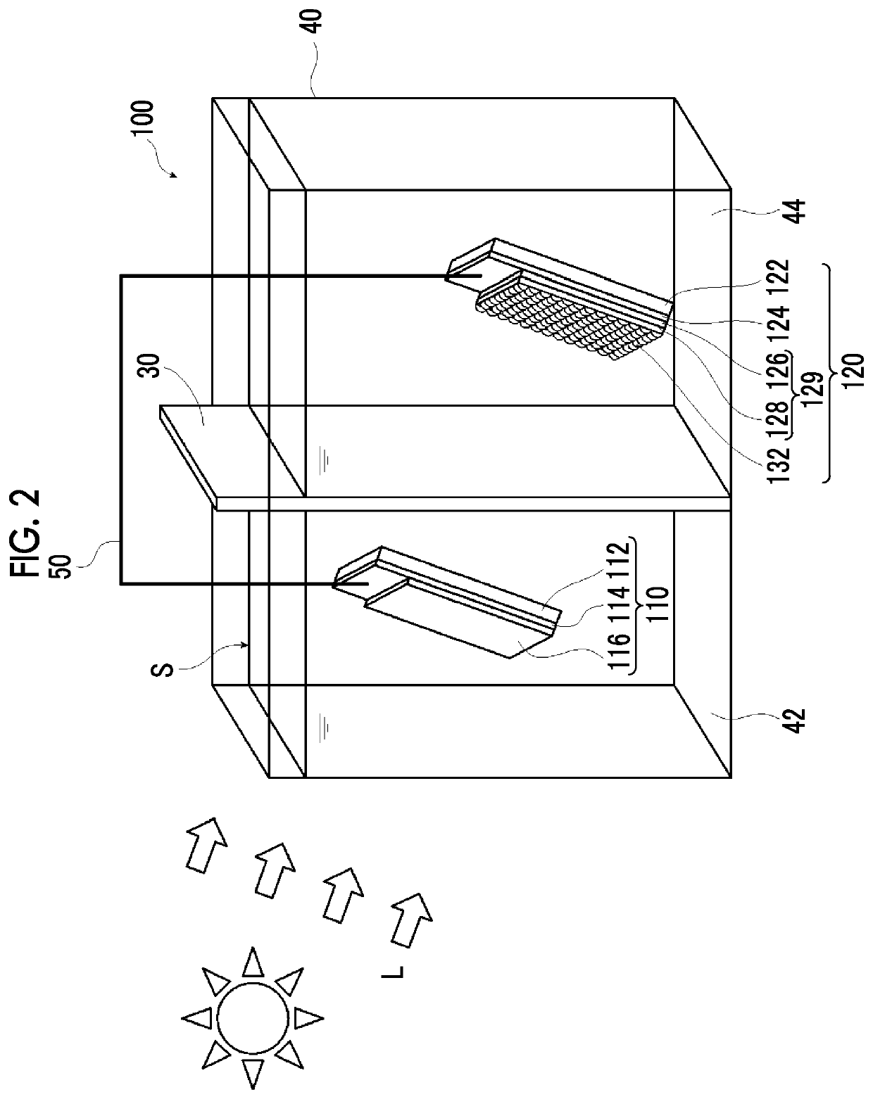
[0141]In one embodiment of a water splitting device of the present invention, the water splitting device generates gases from a photocatalytic electrode for hydrogen generation and a photocatalytic electrode for oxygen generation by irradiating the photocatalytic electrode for hydrogen generation and the photocatalytic electrode for oxygen generation with light, and includes a bath to be filled with an electrolytic aqueous solution and the photocatalytic electrode for hydrogen generation and the photocatalytic electrode for oxygen generation each disposed in the bath, in which the photocatalytic electrode for hydrogen generation has a p-type semiconductor layer, an n-type semiconductor layer provided on the p-type semiconductor layer, and a co-catalyst provided on the n-type semiconductor layer, and a band offset ΔE which is a difference between a potential p-CBM at a lower end of a conduction band of the p-type semiconductor layer and a potential n-CBM at a lower end of a conductio...

example 1

[0149]A photocatalytic electrode of Example 1 was produced as follows.

[0150]First, a layer (conductive layer) having a thickness of 600 nm and formed of Mo was formed on the surface of a soda-lime glass substrate (insulating substrate) by a direct current (DC) magnetron sputtering method using a magnetron sputtering apparatus (product name “CFS-12P”, manufactured by Shibaura Eletech Corporation).

[0151]Next, a layer (p-type semiconductor layer) formed of a CIGS compound semiconductor having a thickness of 2 μm was formed on the surface of the conductive layer by a three-step method using a multi-source vapor deposition apparatus (product name “EW-10”, manufactured by EIKO Engineering Corporation). Specifically, Cu, In, Ga, and Se were used as vapor deposition sources, the substrate temperature of the first step was set to 400° C., and the substrate temperatures of the second and third steps were set to 520° C. The Ga ratio (Ga / (Ga+In)) was adjusted by controlling the vapor deposition...


PUM

PropertyMeasurementUnit
molar ratioaaaaaaaaaa
voltageaaaaaaaaaa
molar ratioaaaaaaaaaa

Abstract

An object of the present invention is to provide a photocatalytic electrode for water splitting and a water splitting device excellent in the onset potential. The water splitting device of the present invention is a water splitting device which generates gases from a photocatalytic electrode for hydrogen generation and a photocatalytic electrode for oxygen generation by irradiating the photocatalytic electrode for hydrogen generation and the photocatalytic electrode for oxygen generation with light, and includes a bath to be filled with an electrolytic aqueous solution and the photocatalytic electrode for hydrogen generation and the photocatalytic electrode for oxygen generation each disposed in the bath. The photocatalytic electrode for hydrogen generation has a p-type semiconductor layer, an n-type semiconductor layer provided on the p-type semiconductor layer, and a co-catalyst provided on the n-type semiconductor layer. The p-type semiconductor layer is a semiconductor layer containing a CIGS compound semiconductor containing Cu, In, Ga, and Se, and a molar ratio of Ga to a total molar amount of Ga and In in the CIGS compound semiconductor is 0.4 to 0.8.

Description

CROSS-REFERENCE TO RELATED APPLICATIONS[0001]This application is a Continuation of PCT International Application No. PCT / JP2019 / 007233 filed on Feb. 26, 2019, which claims priority under 35 U.S.C. § 119(a) to Japanese Patent Application No. 2018-040134 filed on Mar. 6, 2018. The above application is hereby expressly incorporated by reference, in its entirety, into the present application.BACKGROUND OF THE INVENTION1. Field of the Invention[0002]The present invention relates to a photocatalytic electrode for water splitting and a water splitting device.2. Description of the Related Art[0003]It is known that a CIGS compound formed of an alloy of Cu, In, Ga, and Se is used as a light absorbing layer of a solar battery, due to the fact that it has excellent sunlight conversion efficiency. For example, Phys. Status Solidi RRL 10, No. 8, 583-586 (2016) / DOI 10.1002 / pssr. 201600199 discloses that in a case where the molar ratio of Ga to the total amount of Ga and In is 0.3 as a CIGS compoun...

Claims


Application Information

Patent Timeline
Patent Type & Authority Applications(United States)
IPC IPC(8): C25B1/00C25B9/06C25B1/04C25B11/04B01J35/00C25B9/17
CPCC25B9/06C25B11/0473C25B1/003C25B11/0415C25B1/04C25B11/0405B01J27/04B01J27/057C01B3/04C01B3/02C01B13/02Y02E60/36C25B11/049C25B9/50B01J35/00B01J35/30C25B1/55C25B9/17C25B11/051C25B11/057C25B11/081
Inventor KOBAYASHI, HIROYUKIORITA, MASAHIRO
Owner FUJIFILM CORP
Learn More