Method of forming metal nitride film by chemical vapor deposition and method of forming metal contact and capacitor of semiconductor device using the same

a technology of metal nitride and chemical vapor deposition, which is applied in the direction of chemical vapor deposition coating, coating, capacitor, etc., can solve the problems of high-integration semiconductor devices that cannot be applied, the deposition temperature of 600.degree. c. or more exceeds the thermal budget and thermal stress limits of an underlayer

a technology of metal nitride and chemical vapor deposition, which is applied in the direction of chemical vapor deposition coating, coating, capacitor, etc., can solve the problems of high-integration semiconductor devices that cannot be applied, the deposition temperature of 600.degree. c. or more exceeds the thermal budget and thermal stress limits of an underlayer

US6348376B2Inactive Publication Date: 2002-02-19SAMSUNG ELECTRONICS CO LTD

Image

  • Method of forming metal nitride film by chemical vapor deposition and method of forming metal contact and capacitor of semiconductor device using the same
  • Method of forming metal nitride film by chemical vapor deposition and method of forming metal contact and capacitor of semiconductor device using the same
  • Method of forming metal nitride film by chemical vapor deposition and method of forming metal contact and capacitor of semiconductor device using the same

Examples


Embodiment Construction

>

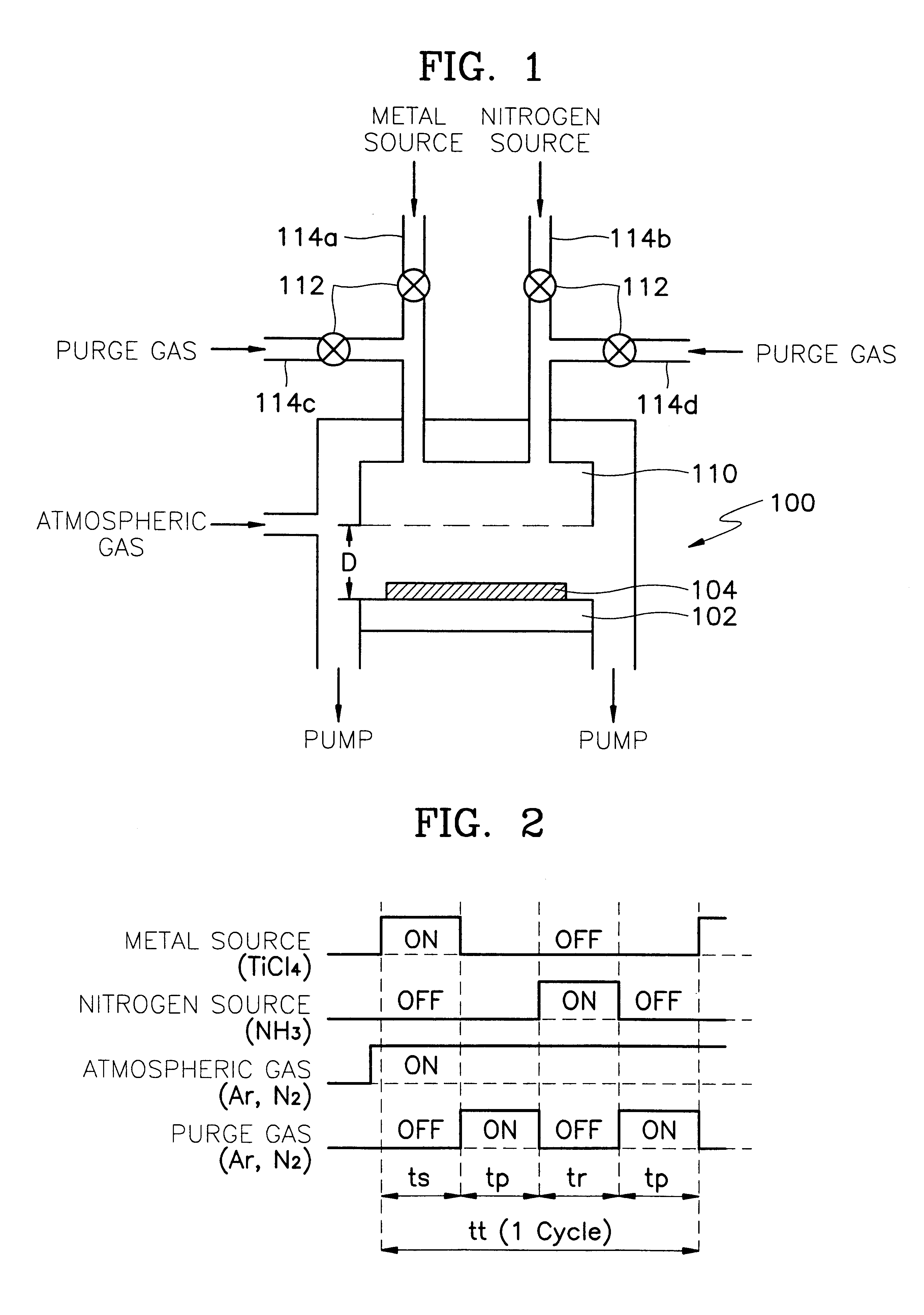
A TiN film is deposited by the cycles comprising the gas pulsing steps, under the following reaction conditions, on the semiconductor substrate 104 which is maintained at a temperature of 500.degree. C. or lower by the heater 102 of FIG. 1.

Deposition Conditions

object material: TiN

atmospheric gas: Ar

pressure in deposition chamber: 1-20Torr

metal source, nitrogen source: TiCl.sub.4, NH.sub.3

flow amount of TiCl.sub.4, pulsing time (t.sub.s) of TiCl.sub.4 :1-5 sccm, 5 sec

flow amount of NH.sub.3, pulsing time (t.sub.r) of NH.sub.3 : 5-30 sccm, 5 sec

purge gas, flow amount of purge gas, purge time (t.sub.p): Ar, 10-100 sccm, 10 sec

carrier gas, flow amount of carrier gas: Ar, 10-100 sccm

time (t.sub.t) for one cycle: 30 sec

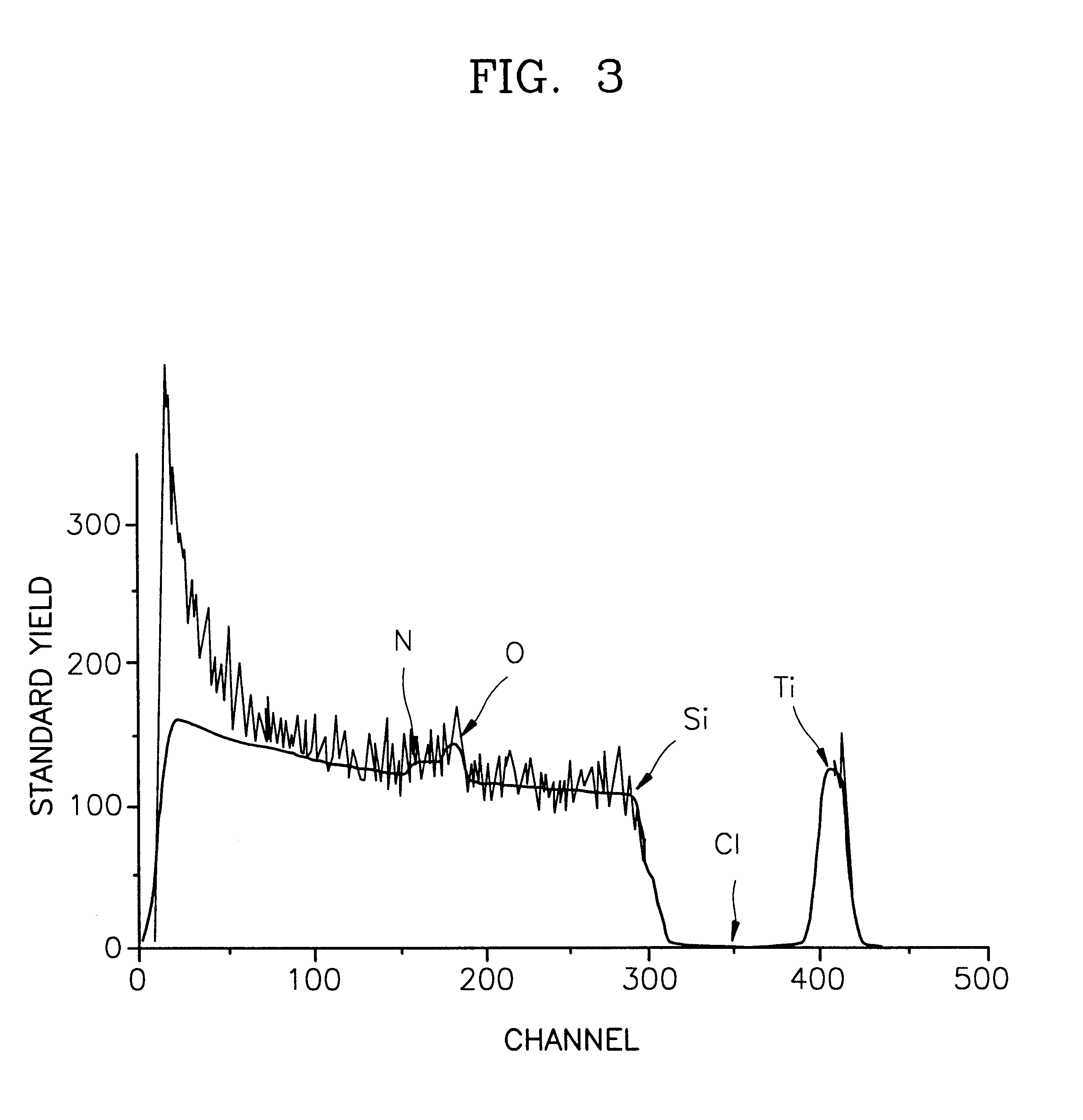
FIG. 3 shows the results of checking the state of the TiN thin film deposited on the semiconductor substrate 104 under the aforementioned conditions using an RBS method. In FIG. 3, a horizontal axis indicates channels in a multi-channel analyzer (MCA), and a vertical axis ...


PUM

PropertyMeasurementUnit
pressureaaaaaaaaaa
temperatureaaaaaaaaaa

Abstract

A method of forming a metal nitride film using chemical vapor deposition (CVD), and a method of forming a metal contact and a semiconductor capacitor of a semiconductor device using the same, are provided. The method of forming a metal nitride film using chemical vapor deposition (CVD) in which a metal source and a nitrogen source are used as a precursor, includes the steps of inserting a semiconductor substrate into a deposition chamber, flowing the metal source into the deposition chamber, removing the metal source remaining in the deposition chamber by cutting off the inflow of the metal source and flowing a purge gas into the deposition chamber, cutting off the purge gas and flowing the nitrogen source into the deposition chamber to react with the metal source adsorbed on the semiconductor substrate, and removing the nitrogen source remaining in the deposition chamber by cutting off the inflow of the nitrogen source and flowing the purge gas into the deposition chamber. Accordingly, the metal nitride film having low resistivity and a low content of Cl even with excellent step coverage can be formed at a temperature of 500° C. or lower, and a semiconductor capacitor having excellent leakage current characteristics can be manufactured. Also, a deposition speed, approximately 20 A / cycle, is suitable for mass production.

Description

1. Field of the InventionThe present invention relates to a method of fabricating semiconductor devices, and more particularly, to a method of forming a metal nitride film by chemical vapor deposition (CVD) where a metal source and a nitrogen source are used as a precursor, and a method of forming a metal contact and a capacitor of a semiconductor device using the above method.2. Description of the Related ArtA barrier metal layer, which prevents mutual diffusion or chemical reaction between different materials, is indispensable to stabilize the contact interfaces of semiconductor devices. In general, a metal nitride such as TiN, TaN or WN has been widely used as the barrier metal layer of semiconductor devices. Here, TiN is a representative example among the above metal nitrides.However, when the metal nitride film such as TiN is fabricated by sputtering, its application to highly integrated semiconductor devices is not appropriate, due to low step coverage. For an example, FIGS. 9...

Claims


Application Information

Patent Timeline
19 Feb 2002
Publication
US6348376B2
IPC
C23C16/34; H01L21/02; H01L21/285; H01L21/70; H01L21/768; C23C16/04; C23C16/44; C23C16/455
CPC
C23C16/34; C23C16/45553; H01L21/28562; H01L21/76804; H01L21/76843; H01L28/91
Inventors
LIM, HYUN-SEOK; KANG, SANG-BOM