Sliding member
- Summary
- Abstract
- Description
- Claims
- Application Information
AI Technical Summary
Benefits of technology
Problems solved by technology
Method used
Image

Examples
examples
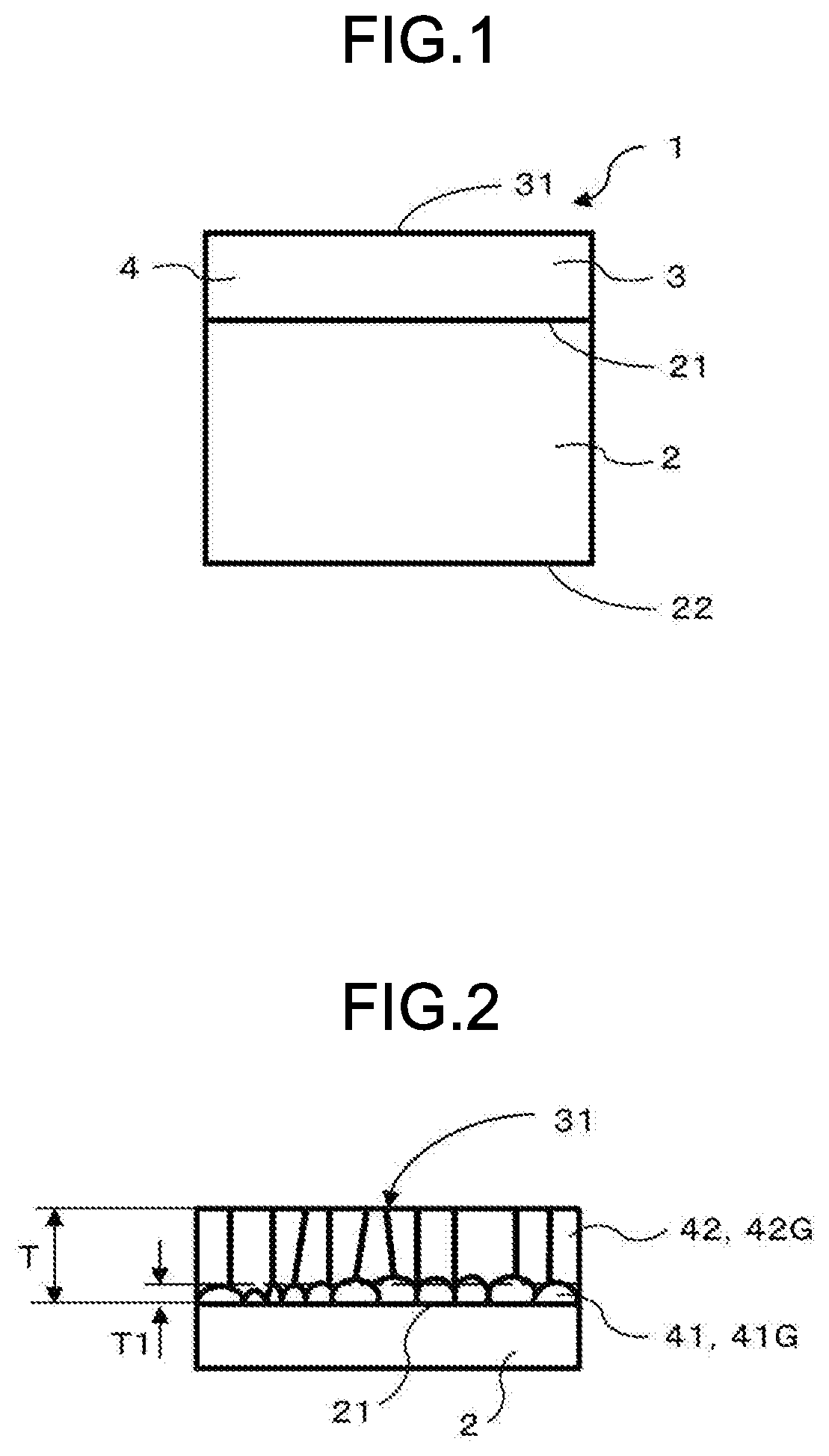
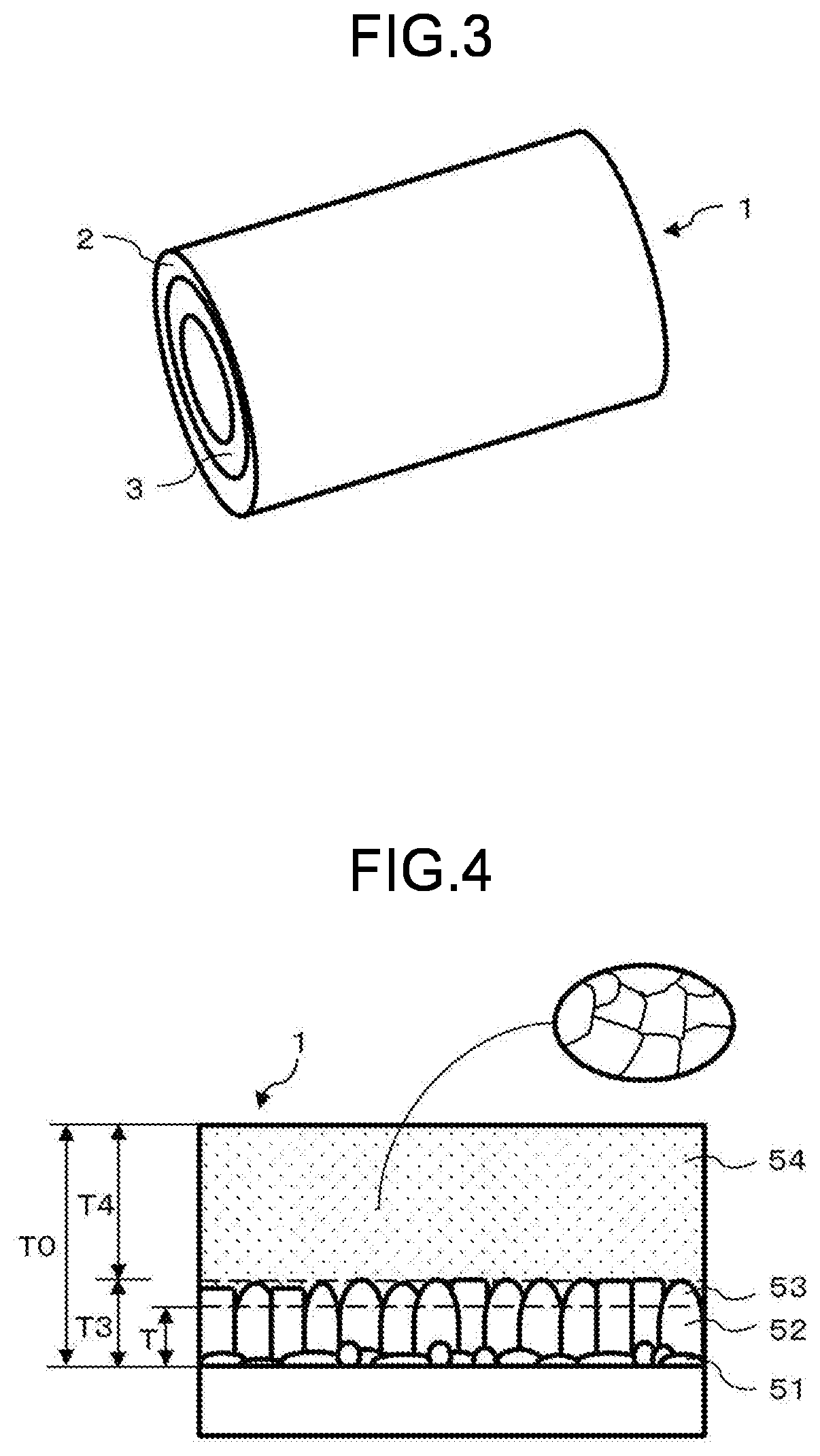
[0047]Samples of Examples 1 to 12 of the sliding member according to the present invention and Comparative Examples 21 to 25 were produced in the following manner. In the production of these samples, a back-metal layer was formed of a cylindrical member of hypoeutectoid steel including 0.2 mass % of carbon. In Examples 1 to 12, a copper alloy having a predetermined composition was melted to obtain a molten copper alloy and poured onto the back-metal layer (inner surface of the cylindrical member) by centrifugal casting process as described above. After casting, the copper alloy layer was subjected to cutting processing, and then subjected to annealing treatment at a temperature of 300° C. for 5 hours to produce a sliding member. The samples were produced to have the same size of an inner diameter of 80 mm, a thickness of 6 mm, and an axial length of 80 mm to be subjected to a sliding test described later.
[0048]In a column “Thickness” in Table 1, a column “Sliding layer thickness T (...
PUM
| Property | Measurement | Unit |
|---|---|---|
| Percent by mass | aaaaa | aaaaa |
| Percent by mass | aaaaa | aaaaa |
| Percent by mass | aaaaa | aaaaa |
Abstract
Description
Claims
Application Information
 - R&D
- Intellectual Property
- Life Sciences
- Materials
- Tech Scout
- Unparalleled Data Quality
- Higher Quality Content
- 60% Fewer Hallucinations
Browse by: Latest US Patents, China's latest patents, Technical Efficacy Thesaurus, Application Domain, Technology Topic, Popular Technical Reports.
© 2025 PatSnap. All rights reserved.Legal|Privacy policy|Modern Slavery Act Transparency Statement|Sitemap|About US| Contact US: help@patsnap.com