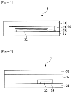
Method for preparing organic electronic device
a technology of electronic devices and organic materials, applied in the direction of semiconductor devices, photovoltaic energy generation, electrical apparatus, etc., can solve the problems of high environmental factor sensitive products comprising oleds, poor etc., and achieve the effect of minimizing the amount of out-gas occurring and excellent flatness of sealing films
- Summary
- Abstract
- Description
- Claims
- Application Information
AI Technical Summary
Benefits of technology
Problems solved by technology
Method used
Image

Examples
example 2
[0082]An organic electronic device was prepared in the same manner as in Example 1, except that the applied ink composition was subjected to heat treatment at 25° C. for 3 minutes, and further heat treatment at 60° C. for 30 minutes after curing.
[0083]EXAMPLE 3
[0084]An organic electronic device was prepared in the same manner as in Example 1, except that the applied ink composition was subjected to heat treatment at 30° C. for 10 minutes, and further heat treatment at 150° C. for 3 minutes after curing.
example 4
[0085]An organic electronic device was prepared in the same manner as in Example 1, except that the applied ink composition was subjected to heat treatment at 25° C. for 3 minutes before curing.
example 5
[0086]An organic electronic device was prepared in the same manner as in Example 1, except that the applied ink composition was subjected to heat treatment at 60° C. for 10 minutes, and further heat treatment at 200° C. for 10 minutes after curing.
PUM
| Property | Measurement | Unit |
|---|---|---|
| wavelength | aaaaa | aaaaa |
| temperature | aaaaa | aaaaa |
| temperature | aaaaa | aaaaa |
Abstract
Description
Claims
Application Information